Method for realizing ultra-narrowband absorption and sensing by utilizing structural symmetry breaking

An ultra-narrow-band, light-absorbing technology, applied in optical components, optics, instruments, etc., can solve problems such as the enhancement of light absorption efficiency, and achieve the effect of high-sensitivity refractive index sensing and ultra-narrow-band selective perfect absorption

Active Publication Date: 2019-08-16
JIANGNAN UNIV
View PDF2 Cites 16 Cited by
  • Summary
  • Abstract
  • Description
  • Claims
  • Application Information

AI Technical Summary

Problems solved by technology

[0003] However, the light absorption enhancement achieved by surface plasmon resonance, guided mode resonance, magnetic resonance, and Fano resonance in the past rarely involves how to use the symmetry breaking of the micro-nano structure to enhance the light absorption efficiency, especially How to Achieve Perfect Light Absorption in an Ultra-Narrow Band
Although recent studies have found that some new optical phenomena and device functions can be realized by using the symmetry breaking of microstructures, such as the use of symmetry breaking of micro-nano structures to produce Fano resonance, electromagnetically induced transparency, narrow-band filtering and enhanced surface plasmons. Bulk resonance, etc., but the above methods are aimed at the resonance, reflection, transmission or filtering characteristics of symmetry-breaking micro-nano structures, and do not involve the use of symmetry breaking in micro-structures to achieve ultra-narrow-band perfect light absorption and high-performance sensing applications

Method used


Image

  • Method for realizing ultra-narrowband absorption and sensing by utilizing structural symmetry breaking
  • Method for realizing ultra-narrowband absorption and sensing by utilizing structural symmetry breaking
  • Method for realizing ultra-narrowband absorption and sensing by utilizing structural symmetry breaking

Examples


Embodiment 1

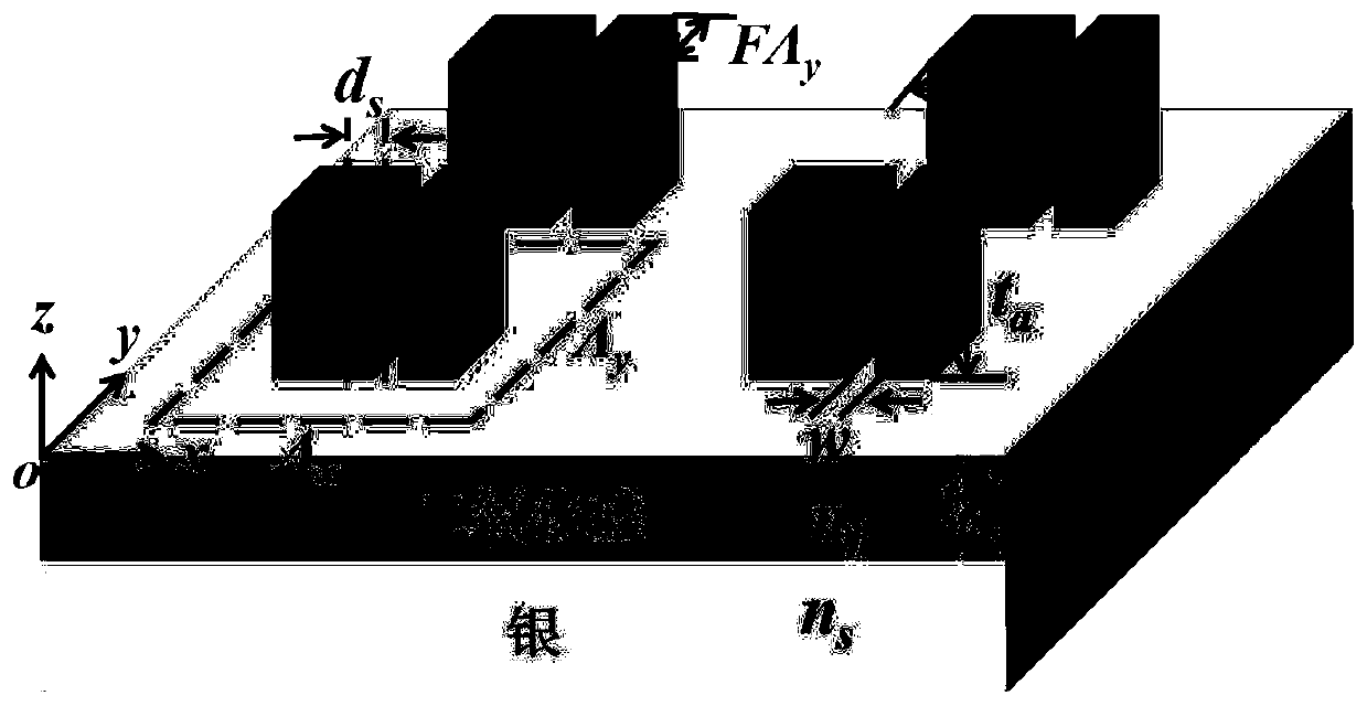
[0026] In the present invention, metal and dielectric film materials can be arbitrarily selected to realize ultra-narrow-band perfect light absorption with symmetry breaking. feel. Firstly, nano-grooves are introduced into the grating structure with a metal substrate. By making the distance between the center of the nano-groove and the center of the original cell of the grating ≠ 0, the symmetry of the grating structure is broken, and the symmetry of the grating structure is used. The highly localized and significantly enhanced light field in the nanogroove is realized, thereby obtaining ultra-narrow-band light absorption and high-sensitivity sensing.

[0027] figure 1 It is a schematic diagram of a two-dimensional grating structure with a metal substrate and nanogrooves. The substrate is a metal with a refractive index n s . Above the substrate is a layer of thickness t b The low refractive index dielectric buffer layer, the refractive index n b . Above the buffer laye...

Embodiment 2

[0031] In order to reveal the physical mechanism corresponding to the ultra-narrow-band light absorption of the symmetry-breaking structure, the rigorous coupled-wave theory is used to calculate the symmetry cases (d s = 0) and the symmetry breaking case (d s ≠0), the electric field distribution of the grating structure at the resonant absorption wavelength of 1455.8nm, we get image 3 .

[0032] image 3 For the structure of the present invention in the symmetrical case (d s = 0) and the symmetry breaking case (d s ≠0), the normalized electric field amplitude distribution of the 1455.8nm absorption peak light wave on the xoy plane. From image 3 It can be seen that for a symmetric structured grating, that is, d s = 0, w = 0 (symmetrical and no nanogrooves), and d s =0, w=20nm (symmetrical and with nano-grooves), regardless of whether there are nano-grooves in the grating, due to the local effect of the high-refractive index grating on the light field, although the elec...

Embodiment 3

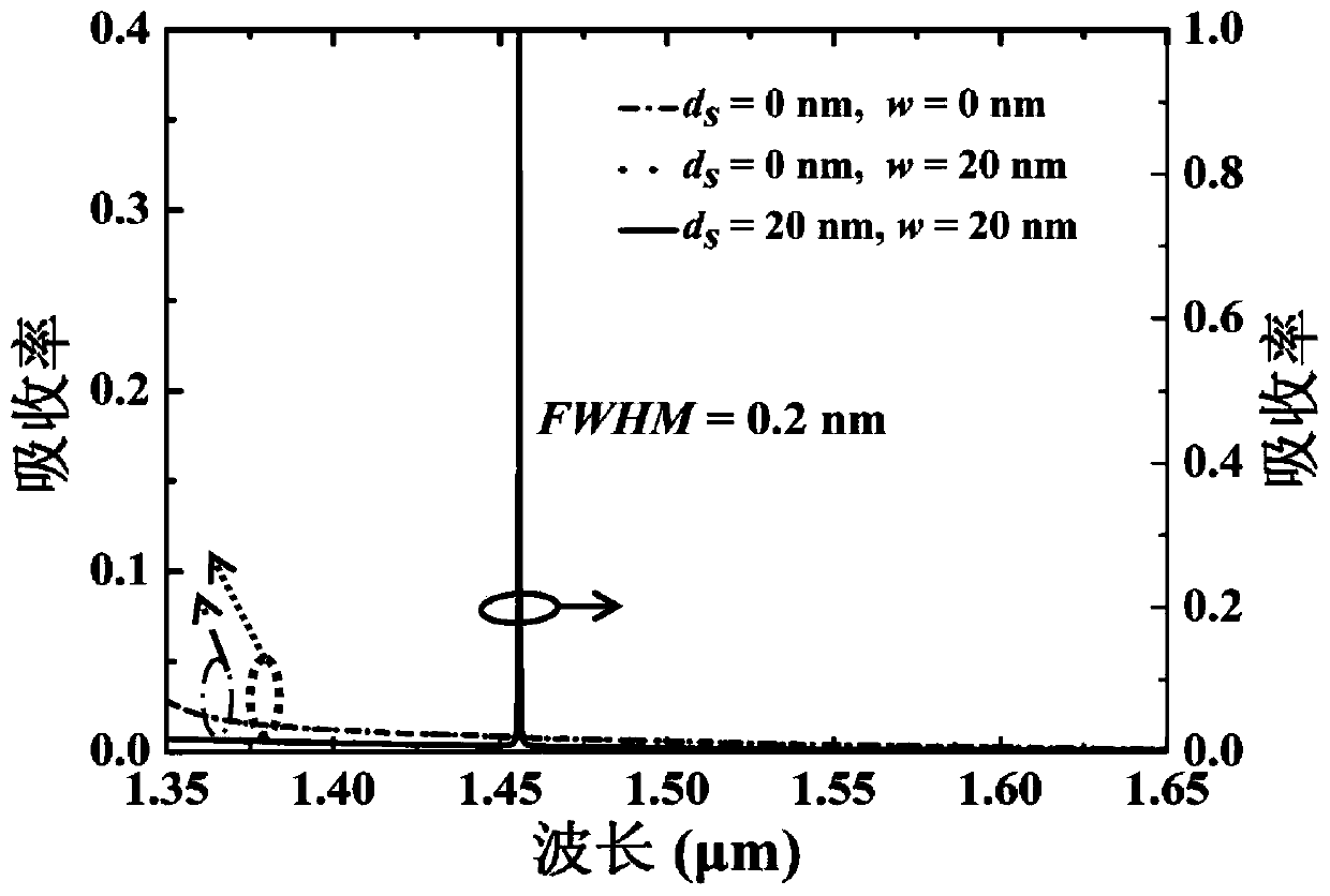
[0034] For the symmetry-breaking grating structure (d s ≠0), under the condition of groove width w=20nm, select different groove positions d s , such as d s take d respectively s =20nm,d s =30nm, d s = 40nm, d s = 50nm, d s =60nm, d can be calculated using vector diffraction theory s The absorption spectrum curve of the structure when it changes;

[0035] Depend on Figure 4 It can be seen that when d s When increasing from 20nm to 60nm, the ultra-narrow band absorption peak has a significant red shift, and the absorption peak wavelength moves from 1455.8nm to 1498.1nm, that is, as the asymmetry of the grating structure increases (that is, the d s ), the narrow-band absorption peak moves to the long-wave direction, but the corresponding low-absorption sideband remains unchanged, and the structure still maintains excellent ultra-narrow-band selective absorption characteristics.


PUM


Abstract

The invention discloses a method for realizing ultra-narrowband absorption and sensing by utilizing structural symmetry breaking, and belongs to the field of microelectromechanical systems and photoelectric detection. A grating structure of the invention is composed of a metal substrate, a dielectric buffer layer with a low refractive index and a dielectric grating layer with a high refractive index, a nano-groove is introduced into the grating layer, the symmetry of the grating structure is changed by changing the position of the nano-groove, the high locality and significant enhancement of alight field in the nano-groove are achieved by using the symmetry breaking of the grating structure, and then ultra-narrowband selective absorption of incident light waves is realized. In addition, since the electric field energy is highly localized in the nano-groove of the symmetry breaking grating, a small change in the background refractive index will cause significant movement of an absorption peak, the method can be used for achieving a high-sensitivity refractive index sensing function at the same time, and thus has an application value in such fields as light absorption devices, enhanced nano imaging, stealth materials, photoelectric detection, biosensing, and so on.

Description

technical field [0001] The invention relates to a method for realizing ultra-narrow band absorption and sensing by using structural symmetry breaking, and belongs to the field of micro-electromechanical systems and photoelectric detection. Background technique [0002] Optically selective perfect absorbers can efficiently absorb electromagnetic waves in specific frequency bands and achieve perfect absorption of light wave energy in specific channels. They have important application requirements in the fields of photoelectric detection, optical sensing, imaging systems, intelligent communications, and photovoltaic solar energy. For micro-nano optical devices, in order to achieve a good light absorption effect, it is often necessary to increase the interaction between the incident light wave and the micro-nano structure, and use the electric field enhancement of the micro-nano structure to improve the light absorption efficiency of the device. In previous studies and applicati...

Claims


Application Information

Patent Timeline
Patent Type & Authority Applications(China)
IPC IPC(8): G02B5/00
CPCG02B5/003
Inventor 桑田尹欣齐红龙李国庆王勋
Owner JIANGNAN UNIV
Why Eureka
Try Eureka