Photoresist, its preparation method, application and modification method of medical material surface
A photoresist and matrix material technology, applied in the field of biomedical materials, can solve the problems of influence, high price, decomposition or coating function damage, etc., and achieve the effect of reducing costs, reducing steps, and good biodescriptivity
- Summary
- Abstract
- Description
- Claims
- Application Information
AI Technical Summary
Problems solved by technology
Method used
Image

Examples
Embodiment 1
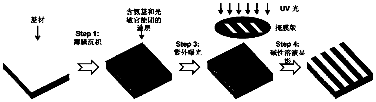
[0041]This embodiment provides a new type of photoresist, which includes a coating containing both photosensitive functional groups and amino functional groups prepared by plasma chemical vapor deposition. The thickness of the coating is 1 nm, and the precursor is allylamine vapor.
[0042] This embodiment also provides a method for preparing a novel photoresist, comprising the following steps:
[0043] Put the silicon wafer into the vacuum chamber of the plasma polymerization equipment, and pump the vacuum to 0.1Pa, pass in 5sccm argon gas, and perform plasma sputtering cleaning under the conditions of radio frequency power 100W and bias voltage -100V; sputtering cleaning is completed Finally, the vacuum chamber was evacuated to 0.1Pa, and 5sccm allylamine vapor and 2sccm argon gas were introduced to make the working pressure 6Pa; under the conditions of 60W radio frequency power, -50V bias voltage and 20% pulse duty cycle, 10 Minute film deposition, and finally a coating co...
Embodiment 2
[0047] This embodiment provides a new type of photoresist, which includes a coating containing both photosensitive functional groups and amino functional groups prepared by plasma chemical vapor deposition. The thickness of the coating is 1000 nanometers, and the precursor is a mixed gas of ammonia and acetylene.
[0048] This embodiment also provides a method for preparing a novel photoresist, comprising the following steps:
[0049] Put the silicon wafer into the vacuum chamber of the plasma polymerization equipment, and pump the vacuum to 0.1Pa, pass in 5sccm argon gas, and perform plasma sputtering cleaning under the conditions of radio frequency power 100W and bias voltage -100V; sputtering cleaning is completed Finally, the vacuum chamber is evacuated to 0.1Pa, and 2sccm ammonia gas, 1sccm acetylene and 1sccm argon gas are introduced to make the working pressure 5Pa; under the condition that the RF power is 60W, the bias voltage is -50V, and the pulse duty ratio is 20%. ...
Embodiment 3
[0053] This embodiment provides a new type of photoresist, which includes a coating containing both photosensitive functional groups and amino functional groups prepared by plasma chemical vapor deposition. The thickness of the coating is 500 nanometers, and the precursor is a mixed gas of nitrogen, acetylene and hydrogen.
[0054] This embodiment also provides a method for preparing a novel photoresist, comprising the following steps:
[0055] Put the silicon wafer into the vacuum chamber of the plasma polymerization equipment, and pump the vacuum to 0.1Pa, pass in 5sccm argon gas, and perform plasma sputtering cleaning under the conditions of radio frequency power 100W and bias voltage -100V; sputtering cleaning is completed Finally, the vacuum chamber is evacuated to 0.1Pa, and 2sccm nitrogen, 1sccm acetylene, 1sccm hydrogen and 1sccm argon are introduced to make the working pressure 6Pa; the RF power is 60W, the bias voltage is -50V, and the pulse duty cycle is 20%. Thin ...
PUM
| Property | Measurement | Unit |
|---|---|---|
| thickness | aaaaa | aaaaa |
Abstract
Description
Claims
Application Information
 - Generate Ideas
- Intellectual Property
- Life Sciences
- Materials
- Tech Scout
- Unparalleled Data Quality
- Higher Quality Content
- 60% Fewer Hallucinations
Browse by: Latest US Patents, China's latest patents, Technical Efficacy Thesaurus, Application Domain, Technology Topic, Popular Technical Reports.
© 2025 PatSnap. All rights reserved.Legal|Privacy policy|Modern Slavery Act Transparency Statement|Sitemap|About US| Contact US: help@patsnap.com