Color radiant cooler based on Tamm structure
A cooler, TAM's technology, applied in the field of radiation cooling, can solve the problems of complex color control, color sensitivity to incident angle changes, and large color difference of the three primary colors, achieving high color purity, no conflict between color rendering and cooling, and good cooling performance Effect
- Summary
- Abstract
- Description
- Claims
- Application Information
AI Technical Summary
Problems solved by technology
Method used
Image
Examples
Embodiment 1
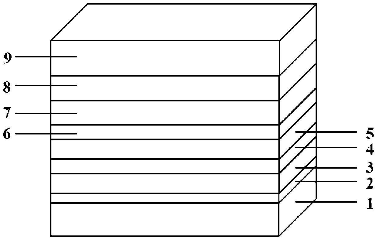
[0037] A yellow radiation cooler based on the Tam structure, the preparation method is as follows:
[0038] S1) Select a piece of SiO after ion beam cleaning 2 For the glass base layer, use electron beam evaporation technology to deposit Ag metal film layer with a thickness of 24nm;
[0039] S2) Then use radio frequency magnetron reactive sputtering technology to deposit a SiC dielectric layer A with a thickness of 30nm on the metal film layer, perform 15min pre-sputtering before film deposition, then deposit a SiC film at room temperature, and finally perform high temperature annealing treatment;
[0040] S3) Deposit MgF with a thickness of 56 nm on dielectric layer A using electron beam evaporation technique 2 Dielectric layer B, evaporation background vacuum degree is 2×10 -4 Pa;
[0041] S4) Then use radio frequency magnetron reactive sputtering technology to deposit a SiC dielectric layer C with a thickness of 30nm on the dielectric layer B, and the sputtering method i...
Embodiment 2
[0047] A magenta radiation cooler based on a Tam structure, the preparation method of which is as follows:
[0048] S1) Select a piece of SiO after ion beam cleaning 2 For the glass base layer, use electron beam evaporation technology to deposit Ag metal film layer with a thickness of 22nm;
[0049] S2) Then use radio frequency magnetron reactive sputtering technology to deposit a SiC dielectric layer A with a thickness of 38 nm on the metal film layer. Pre-sputter for 15 minutes before film deposition, then deposit SiC film at room temperature, and finally perform high-temperature annealing treatment;
[0050] S3) Deposit MgF with a thickness of 72 nm on dielectric layer A using electron beam evaporation technique 2 Dielectric layer B, evaporation background vacuum degree is 2×10 -4 Pa;
[0051] S4) Then use radio frequency magnetron reactive sputtering technology to deposit a SiC dielectric layer C with a thickness of 38nm on the dielectric layer B, and the sputtering me...
Embodiment 3
[0057] A cyan radiation cooler based on a Tam structure, the preparation method of which is as follows:
[0058] S1) Select a piece of SiO after ion beam cleaning 2 For the glass base layer, use electron beam evaporation technology to deposit Ag metal film layer with a thickness of 23nm;
[0059] S2) Then use radio frequency magnetron reactive sputtering technology to deposit a SiC dielectric layer A with a thickness of 47 nm on the metal film layer. Pre-sputter for 15 minutes before film deposition, then deposit SiC film at room temperature, and finally perform high-temperature annealing treatment;
[0060] S3) Deposit MgF with a thickness of 88nm on dielectric layer A using electron beam evaporation technique 2 Dielectric layer B, evaporation background vacuum degree is 2×10 -4 Pa;
[0061] S4) Then use radio frequency magnetron reactive sputtering technology to deposit a SiC dielectric layer C with a thickness of 47nm on the dielectric layer B, and the sputtering method...
PUM
| Property | Measurement | Unit |
|---|---|---|
| thickness | aaaaa | aaaaa |
| thickness | aaaaa | aaaaa |
| thickness | aaaaa | aaaaa |
Abstract
Description
Claims
Application Information
 - R&D Engineer
- R&D Manager
- IP Professional
- Industry Leading Data Capabilities
- Powerful AI technology
- Patent DNA Extraction
Browse by: Latest US Patents, China's latest patents, Technical Efficacy Thesaurus, Application Domain, Technology Topic, Popular Technical Reports.
© 2024 PatSnap. All rights reserved.Legal|Privacy policy|Modern Slavery Act Transparency Statement|Sitemap|About US| Contact US: help@patsnap.com


