A wide spectral response ingaas single photon avalanche photodiode and its manufacturing method

A single-photon avalanche and photodiode technology, applied in the field of light detection, can solve problems such as difficulty in detecting photons, failure to achieve single-photon sensitivity, and difficulty in realizing charge collection.

Active Publication Date: 2021-11-16
CHONGQING UNIV OF POSTS & TELECOMM
View PDF2 Cites 0 Cited by
  • Summary
  • Abstract
  • Description
  • Claims
  • Application Information

AI Technical Summary

Problems solved by technology

However, after the In composition is increased, the lattice constant of the high-indium composition InGaAs material no longer matches the substrate, and such defects will increase the noise, so that the single-photon sensitivity cannot be achieved
On the other hand, due to the absorption of light waves below 900nm by the substrate, the photogenerated carriers will be recombined quickly in the substrate material, making it difficult to achieve effective charge collection, so it is difficult for devices with this structure to detect light below 900nm. photon

Method used


Image

  • A wide spectral response ingaas single photon avalanche photodiode and its manufacturing method
  • A wide spectral response ingaas single photon avalanche photodiode and its manufacturing method

Examples


Embodiment Construction

[0030] The technical solutions in the embodiments of the present invention will be described clearly and in detail below with reference to the drawings in the embodiments of the present invention. The described embodiments are only some of the embodiments of the invention.

[0031] The technical scheme that the present invention solves the problems of the technologies described above is:

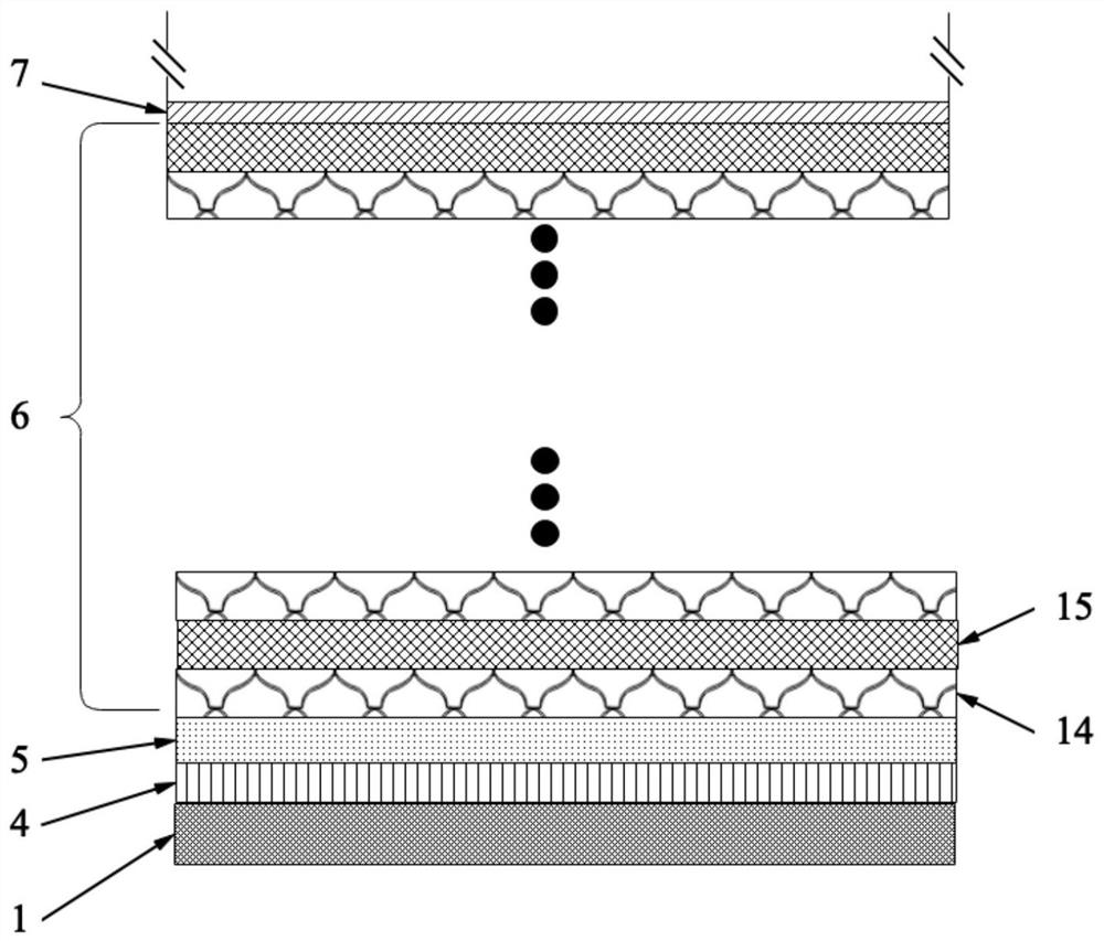
[0032] Such as figure 1 As shown, the present invention is made up of substrate (1) etc., is provided with short-wave light transmission window (2) on described substrate (1), is provided with n electrode (3) on one side of described substrate (1) ), the other side is provided with corrosion cut-off layer (4), InGaAs standard wavelength absorption layer (5), long-wave absorption layer (6), gradient layer (7), charge layer (8), multiplication layer (9) and passivation layer (13). A ladder-type PN junction (10) is arranged inside the multiplication layer (9), and a p-electrode (12) and a pa...


PUM

PropertyMeasurementUnit
diameteraaaaaaaaaa
thicknessaaaaaaaaaa
thicknessaaaaaaaaaa

Abstract

The present invention claims to protect an InGaAs single-photon avalanche photodiode with wide spectral response, including a substrate, a short-wave light transmission window is arranged on the substrate, an n-electrode is arranged on one side of the substrate, and an n-electrode is arranged on the other side. There is a corrosion cut-off layer, and an InGaAs standard wavelength absorption layer, a long-wave absorption layer, a gradient layer, a charge layer, a multiplication layer and a passivation layer are sequentially arranged on the corrosion cut-off layer. A ladder-type PN junction is arranged in the multiplication layer, and a p-electrode and a passivation layer are arranged on the other side of the multiplication layer. The p-electrode, the ladder-type PN junction, and the light-transmitting window are all on the same axis. The invention adopts the long-wave absorbing layer to absorb photons with a wavelength of 1700nm-1800nm, and at the same time prevents the photons in the 760nm-900nm band from being absorbed in the substrate material through the light-transmitting window on the substrate. The response wavelength range of the InGaAs single-photon avalanche photodiode is extended from 900nm-1700nm to 760nm-1800nm, and the detection sensitivity of a single photon is provided in this wavelength range.

Description

technical field [0001] The invention belongs to the technical field of light detection, in particular to an InGaAs single-photon avalanche photodiode with wide spectral response. Background technique [0002] Indium gallium arsenide (InGaAs) single-photon avalanche photodiode is a single-photon detection device based on semiconductor materials, which can detect the energy of a single photon. It has been widely used in quantum communication, true random number generator, laser radar, optical time domain reflectometer and other fields. The working principle of the single-photon avalanche photodiode is: when a photon is absorbed in the diode absorption region, an initial electron-hole pair will be generated, and then under the action of an electric field, the electron or hole will be transported to the multiplication region to generate continuous amplification. As a result, macroscopic electrical signals can be observed. [0003] In terms of spectral response, usually InGaAs ...

Claims


Application Information

Patent Timeline
Patent Type & Authority Patents(China)
IPC IPC(8): H01L31/107H01L31/0304H01L31/02H01L31/0216H01L31/18
CPCH01L31/02H01L31/02161H01L31/03046H01L31/107H01L31/1844
Inventor 王玺黎淼李传波陈伟高新江张承黄超意何丰马勇
Owner CHONGQING UNIV OF POSTS & TELECOMM
Why Eureka
Try Eureka