Inline structure and production process of a thin film photovoltaic module

A thin-film photovoltaic module and laser scribing technology, which is applied in photovoltaic power generation, electrical components, semiconductor devices, etc., can solve the problems of large resistance, shading, and large dead area, and achieve low resistance, simple preparation process, and utilization per unit area. high rate effect

Inactive Publication Date: 2020-11-20
西安富阎移动能源有限公司
View PDF4 Cites 0 Cited by
  • Summary
  • Abstract
  • Description
  • Claims
  • Application Information

AI Technical Summary

Problems solved by technology

[0007] The invention provides an inline structure and production process of a thin film photovoltaic module, which solves the technical problems of shading, excessive dead zone area and large resistance caused by the existing inline structure of photovoltaic modules

Method used


Image

  • Inline structure and production process of a thin film photovoltaic module
  • Inline structure and production process of a thin film photovoltaic module
  • Inline structure and production process of a thin film photovoltaic module

Examples


Embodiment 1

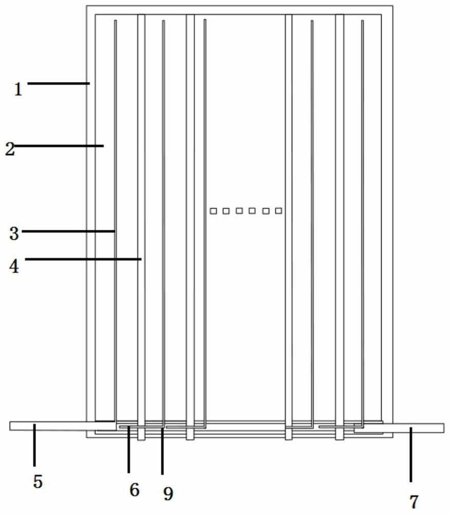
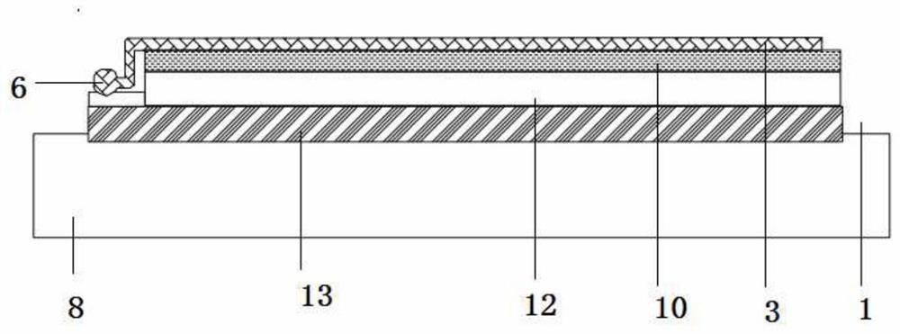
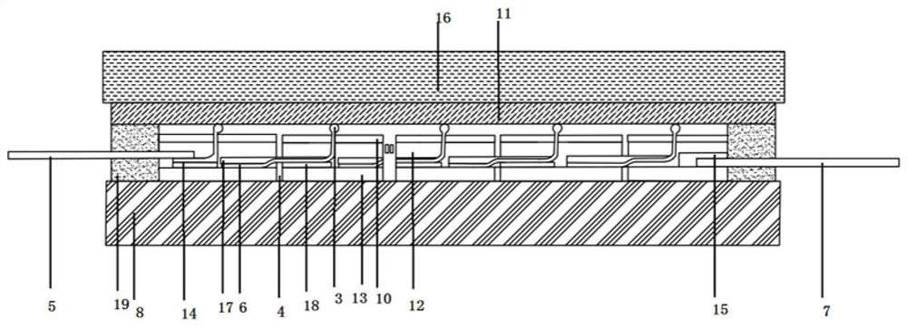
[0030] Example 1, such as figure 1 , figure 2 , image 3 As shown, the inline structure of the thin film photovoltaic module includes a substrate layer 8, a back conductive layer 13, an absorption layer 12, and a transparent conductive layer 10 arranged in sequence from bottom to top, and a laser scribed groove 4 is laser-marked on the thin-film stack The depth of the laser scribed groove 4 reaches the substrate layer 8, which is used to divide the battery into several sub-cells 2. The width of the scribed groove 4 is 25 μm or 150 μm, preferably 100 μm. If the scribed groove 4 is too wide, the dead zone is too large. Too narrow can easily lead to short circuit phenomenon; on the four sides of the battery as a whole, there is an edge laser scribe area 1 that reaches the depth of the substrate layer 8, and the edge laser scribe penetrates the transparent conductive layer 10, the absorption layer 12 and the back conductive layer 13 until the substrate layer 8, so as to effecti...

Embodiment 2

[0034] Embodiment 2, the present invention also provides a production process of the inline structure of the thin film photovoltaic module, comprising the following steps:

[0035] S1 deposits the back conductive layer 13, the absorption layer 12 and the transparent conductive layer 10 sequentially on the substrate layer 8, and the preparation of the entire thin film stack can be deposited continuously, which avoids the frequent contact between each film layer due to air contact during the preparation of each layer of thin film. Contact causes oxidation or contamination, and ensures good bonding between the film layers in a continuous vacuum environment. The substrate layer 8 can be made of materials such as stainless steel, glass or polyester; the back conductive layer 13 is used as the positive electrode of the battery, the transparent conductive layer 10 is used as the negative electrode of the battery, and the absorbing layer 12 is the core absorbing layer of the battery P~...


PUM

PropertyMeasurementUnit
widthaaaaaaaaaa
widthaaaaaaaaaa
diameteraaaaaaaaaa

Abstract

The invention belongs to the technical field of patented photovoltaic modules, and in particular relates to an inline structure and a production process of a thin film photovoltaic module. The inlinestructure comprises a substrate layer, a back conductive layer, an absorbing layer and transparent conductive layers, wherein the whole thin film stack is scribed by laser scribing grooves to form a plurality of sub-cells, edge laser scribing regions are formed around the whole thin film stack, a carrier-collecting metal wire is screen-printed or laid on the transparent conductive layer of each ofthe sub-cells, and a bus bar is used to connect the carrier-collecting metal wires of the adjacent sub-cells with the back conductive layer to form series relationship of the respective sub-cells. Insulating adhesive films are placed on the upper and lower sides of the bus bar to effectively prevent the battery itself from being short-circuited. Therefore, compared with the inline structure of the thin film photovoltaic module in the prior art, the "dead zone" is smaller to make a higher unit area utilization for the thin film photovoltaic module, the resistance is smaller, the process is simpler, and the laser equipment investment is less during the preparation process to be more stable.

Description

technical field [0001] The patent of the present invention relates to the technical field of photovoltaic power generation, and specifically relates to an inline structure and production process of a thin-film photovoltaic module. Background technique [0002] At present, there are two battery connection methods commonly used in the packaging and manufacturing process of photovoltaic modules: inline method and outboard method. The external connection method is usually arranged through discrete battery pieces, and then the external positive and negative electrodes of the metal bus bar are welded, and the packaging is completed after repeated process arrangement and laying; the inline method usually uses laser multiple times to scribe the insulator battery, and then After each laser scribing, other thin film material stacks are deposited, and the connection between cells is completed through conductive oxides and metal electrodes, and then the packaging is completed. [0003]...

Claims


Application Information

Patent Timeline
Patent Type & Authority Patents(China)
IPC IPC(8): H01L31/0463H01L31/0465
CPCH01L31/0463H01L31/0465Y02E10/50
Inventor 陈国栋陈维强陈艳贞
Owner 西安富阎移动能源有限公司
Why Eureka
Try Eureka