Semiconductor power device and preparation method thereof

A technology of power devices and semiconductors, applied in semiconductor devices, semiconductor/solid-state device manufacturing, transistors, etc., can solve problems such as device failure, device parameter fluctuations, device N+ width fluctuations, etc.

Pending Publication Date: 2019-03-05
BYD SEMICON CO LTD +1
View PDF4 Cites 0 Cited by
  • Summary
  • Abstract
  • Description
  • Claims
  • Application Information

AI Technical Summary

Problems solved by technology

[0006] The contact hole process of the IGBT emitter and the VDMOS source usually uses photolithographic selective etching. The inventors found that the distance from the contact hole electrode to the gate polysilicon will be different due to problems such as alignment deviation and line width deviation of the contact hole photolithography. Fluctuations, resulting in fluctuations in the N+ width of the device, causing fluctuations and deviations in device parameters (such as anti-latch capability), especially when the design margin is low, device parameters fluctuate greatly, and even cause device failure

Method used


Image

  • Semiconductor power device and preparation method thereof
  • Semiconductor power device and preparation method thereof
  • Semiconductor power device and preparation method thereof

Examples


Embodiment Construction

[0017] Embodiments of the present invention are described in detail below. The embodiments described below are exemplary only for explaining the present invention and should not be construed as limiting the present invention. If no specific technique or condition is indicated in the examples, it shall be carried out according to the technique or condition described in the literature in this field or according to the product specification. The reagents or instruments used were not indicated by the manufacturer, and they were all commercially available conventional products.

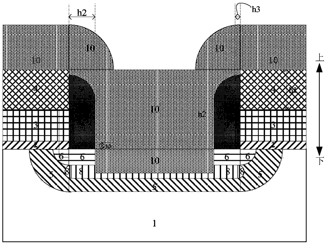
[0018] In one aspect of the invention, the invention provides a semiconductor power device. refer to figure 1 , the semiconductor power device includes: a substrate 1, a groove is arranged in the middle of the substrate 1; a lightly doped well region 5, and the lightly doped well region 5 is arranged in the groove, and covers the inner wall surface of the groove; heavily doped Well region 8, the heavily...


PUM


Abstract

The invention provides a semiconductor power device and a preparation method thereof. The semiconductor power device comprises a substrate, a lightly doped well region, a heavily doped well region, asource region, a gate oxide layer, a gate electrode, a first insulating dielectric layer, a thermal oxide layer, a second insulating dielectric layer and a front-surface metal, wherein the second insulating dielectric layer is disposed above the thermal oxide layer and covers an upper surface of the thermal oxide layer. Therefore, the width of the source region is small, thereby reducing a parasitic resistance under the source region and improving the anti-latching ability; the stability of performance parameters is high and the product yield is high.

Description

technical field [0001] The invention relates to the field of semiconductors, in particular to a semiconductor power device and a preparation method thereof. Background technique [0002] Semiconductor power devices are semiconductor devices capable of handling high voltage and high current. With the rapid development of new power semiconductor devices represented by power MOSFET devices, semiconductor power devices are now widely used. New power semiconductor devices represented by power MOSFETs include VDMOS, LDMOS, and IGBT, etc. VDMOS (vertical double-diffusion MOSFET) is a vertical device, mostly used in discrete devices; LDMOS (Lateral double-diffusion MOSFET) is a horizontal device, its three electrodes are all on the surface of the silicon chip, easy to integrate, and mostly used in the field of power integrated circuits; IGBT (Insulated Gate Bipolar Transistor Insulated Gate Bipolar Transistor), can be regarded as a hybrid new device of power MOS and power BJT. How...

Claims


Application Information

Patent Timeline
Patent Type & Authority Applications(China)
IPC IPC(8): H01L29/78H01L21/336H01L29/739H01L21/331
CPCH01L29/66333H01L29/66712H01L29/7395H01L29/7802
Inventor 郑忠庆
Owner BYD SEMICON CO LTD
Why Eureka
Try Eureka