Tungsten-copper composite electric contact material and preparation method thereof
A technology of contact materials and copper electricity, which is applied in the direction of conductive materials, conductive materials, welding/cutting media/materials, etc., can solve the problem of increasing demand for tungsten-clad copper contact materials, welding adhesion failure, difficult product size consistency, etc. problems, to achieve the effect of improving the yield rate of materials, solving large size differences, and ensuring product size consistency
- Summary
- Abstract
- Description
- Claims
- Application Information
AI Technical Summary
Problems solved by technology
Method used
Image
Examples
preparation example Construction
[0037] A kind of preparation method of tungsten clad copper electric contact material, its raw material comprises tungsten strip material, BAg72Cu strip material and copper strip material, and the widths of the tungsten strip material, BAg72Cu strip material and copper strip material top surface are the same;
[0038] The preparation method comprises the following steps:
[0039] Remove impurities on the surface of raw materials;
[0040] Continuous brazing composite: stack and position the tungsten strip, BAg72Cu strip and copper strip in sequence, so that the tungsten strip, BAg72Cu strip and copper strip are aligned in the width direction and closely bonded, and heated to make the tungsten strip and the copper strip Continuous brazing and compounding of copper strips to obtain tungsten-clad copper strips;
[0041] The tungsten-copper-clad strip is shaped and dot-processed to obtain the above-mentioned tungsten-copper-clad electrical contact material.
[0042] The embodime...
Embodiment 1
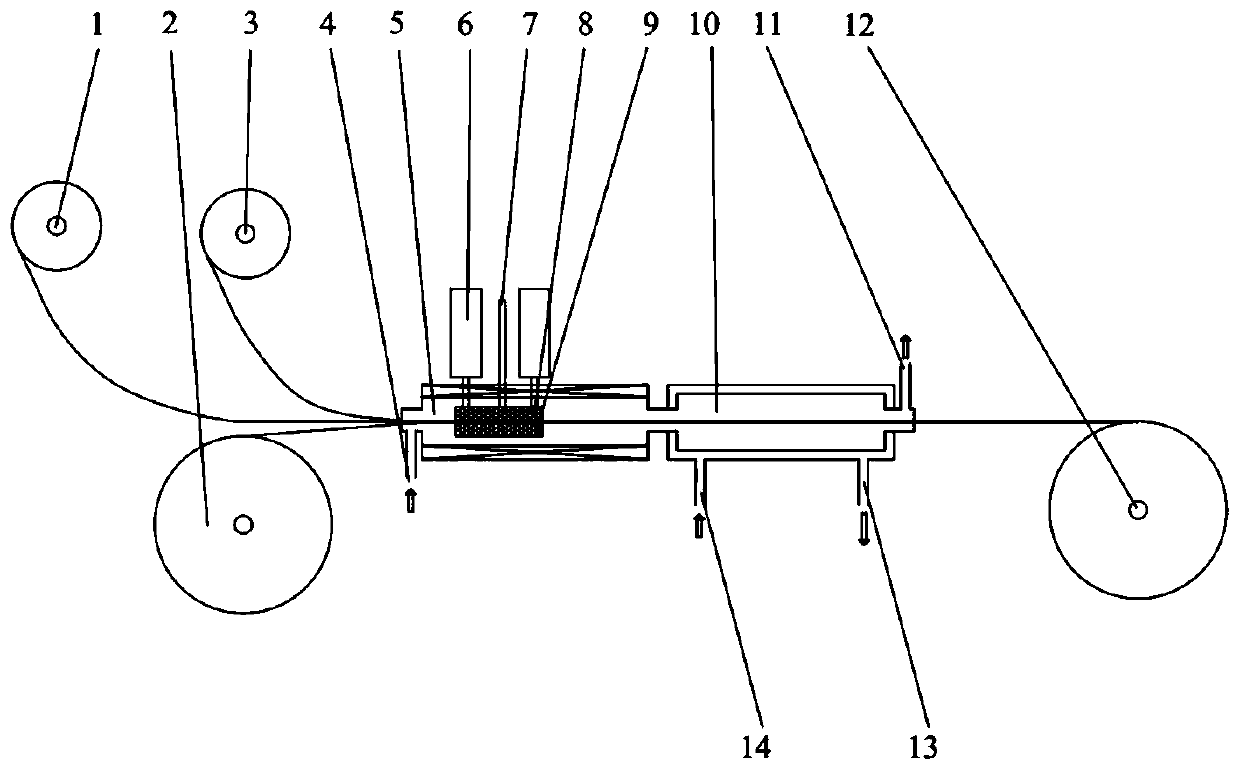
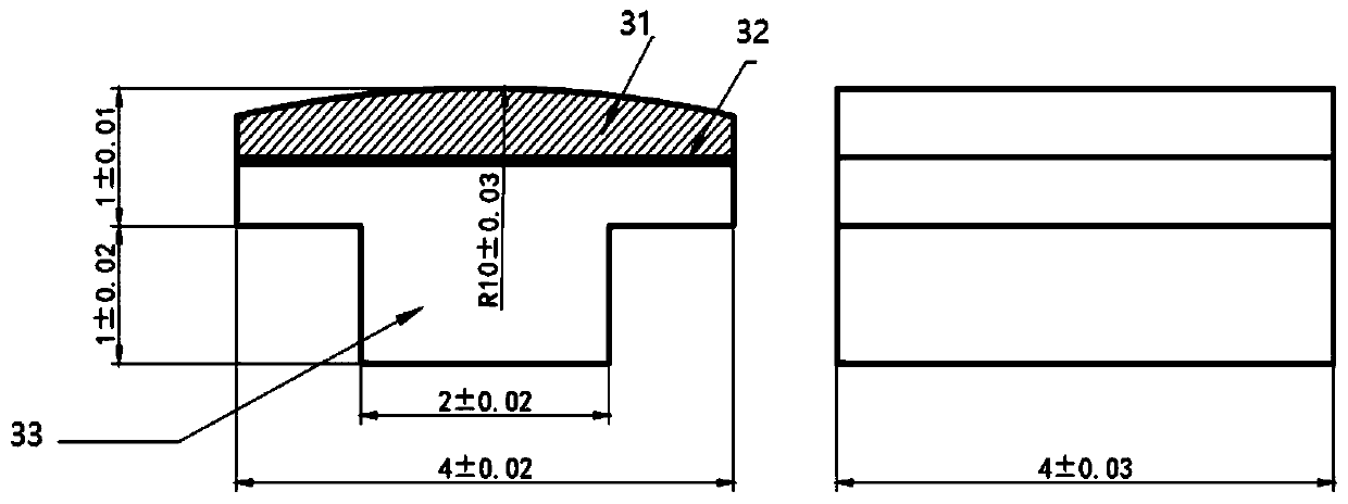
[0057] In this example, W / Cu material T-shaped sheet is prepared, and the specific steps are as follows:
[0058] 1. Purchase of tungsten strips: tungsten strips with specifications of 4mm×0.5mmR×L, prepare tungsten strips 3;
[0059] 2. Preparation of T-shaped copper strip: prepare a right-angled T-shaped TU1 copper strip with a specification of 4mm×0.5mm+2mm×1mm by profile rolling process, and prepare special-shaped copper strip 2;
[0060] 3. Preparation of brazing material strip: BAg72Cu brazing material strip is rolled to a thickness of 0.05±0.01mm, and then slit into a 4mm wide strip on precision slitting equipment, and BAg72Cu brazing material strip 1 is prepared;
[0061] 4. Cleaning before strip brazing: degrease and clean the surfaces of BAg72Cu solder strip 1, special-shaped copper strip 2, and tungsten strip 3;
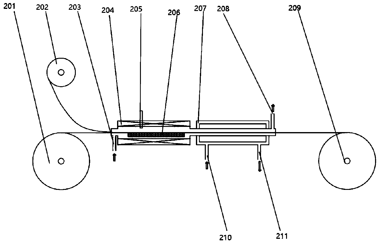
[0062] 5. Continuous brazing compound: First, customize the upper platen 8 of the openable pressure device, and the lower platen 9 of the openable pressu...
Embodiment 2
[0068] This embodiment prepares W / Cu / BAg15CuP profile sheet, the specific steps are as follows:
[0069] 1. Purchase of tungsten strips: tungsten strips with specifications of 3mm×0.5mmR×L, prepare tungsten strips 3;
[0070] 2. Preparation of profiled copper strips: use the profiling process to prepare 3mm×0.5mm TU1 copper profiles with convex ribs, and prepare special-shaped copper strips 2;
[0071] 3. Preparation of solder strips and solder strips: BAg72Cu solder strips are rolled to a thickness of 0.05±0.01mm, then slit into 3mm wide strips on precision slitting equipment, and ready. BAg72Cu solder strips 1; BAg15CuP solder strips The material is purchased with a thickness of 0.03±0.01mm, and then longitudinally cut into a 3mm wide strip, and the BAg15CuP solder strip 202 is prepared.
[0072] 4. Cleaning before strip brazing: degrease and clean the surfaces of BAg72Cu brazing material strip 1, special-shaped copper strip 2, and tungsten strip 3;
[0073] 5. Continuous ...
PUM
| Property | Measurement | Unit |
|---|---|---|
| thickness | aaaaa | aaaaa |
| thickness | aaaaa | aaaaa |
| thickness | aaaaa | aaaaa |
Abstract
Description
Claims
Application Information
 - R&D
- Intellectual Property
- Life Sciences
- Materials
- Tech Scout
- Unparalleled Data Quality
- Higher Quality Content
- 60% Fewer Hallucinations
Browse by: Latest US Patents, China's latest patents, Technical Efficacy Thesaurus, Application Domain, Technology Topic, Popular Technical Reports.
© 2025 PatSnap. All rights reserved.Legal|Privacy policy|Modern Slavery Act Transparency Statement|Sitemap|About US| Contact US: help@patsnap.com


