Display panel and fabrication method thereof

A technology for display panels and preparation steps, which is applied in the manufacture of semiconductor/solid-state devices, electrical components, and electrical solid-state devices, etc., can solve the problems of poor water and oxygen blocking effect, low screen ratio, poor packaging effect of packaging film, etc. The effect of improving screen ratio, prolonging service life and enhancing performance

Active Publication Date: 2019-07-23
WUHAN CHINA STAR OPTOELECTRONICS SEMICON DISPLAY TECH CO LTD
View PDF6 Cites 4 Cited by
  • Summary
  • Abstract
  • Description
  • Claims
  • Application Information

AI Technical Summary

Problems solved by technology

[0006] The purpose of the present invention is to solve the technical problems caused by laser cutting in the existing display panel opening process, such as particle adhesion to the cutting edge, poor effect of blocking water and oxygen, poor encapsulation effect of packaging film layer, and low screen-to-body ratio.

Method used


Image

  • Display panel and fabrication method thereof
  • Display panel and fabrication method thereof
  • Display panel and fabrication method thereof

Examples


Embodiment 1

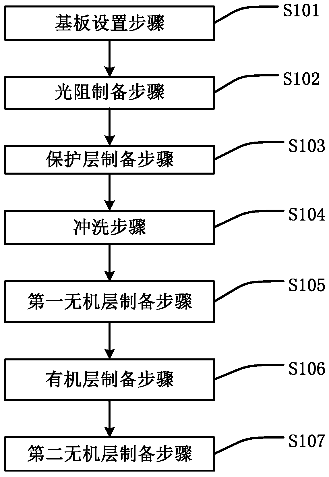
[0044] like figure 1 As shown, this embodiment provides a method for manufacturing a display panel, including steps S101-S107.

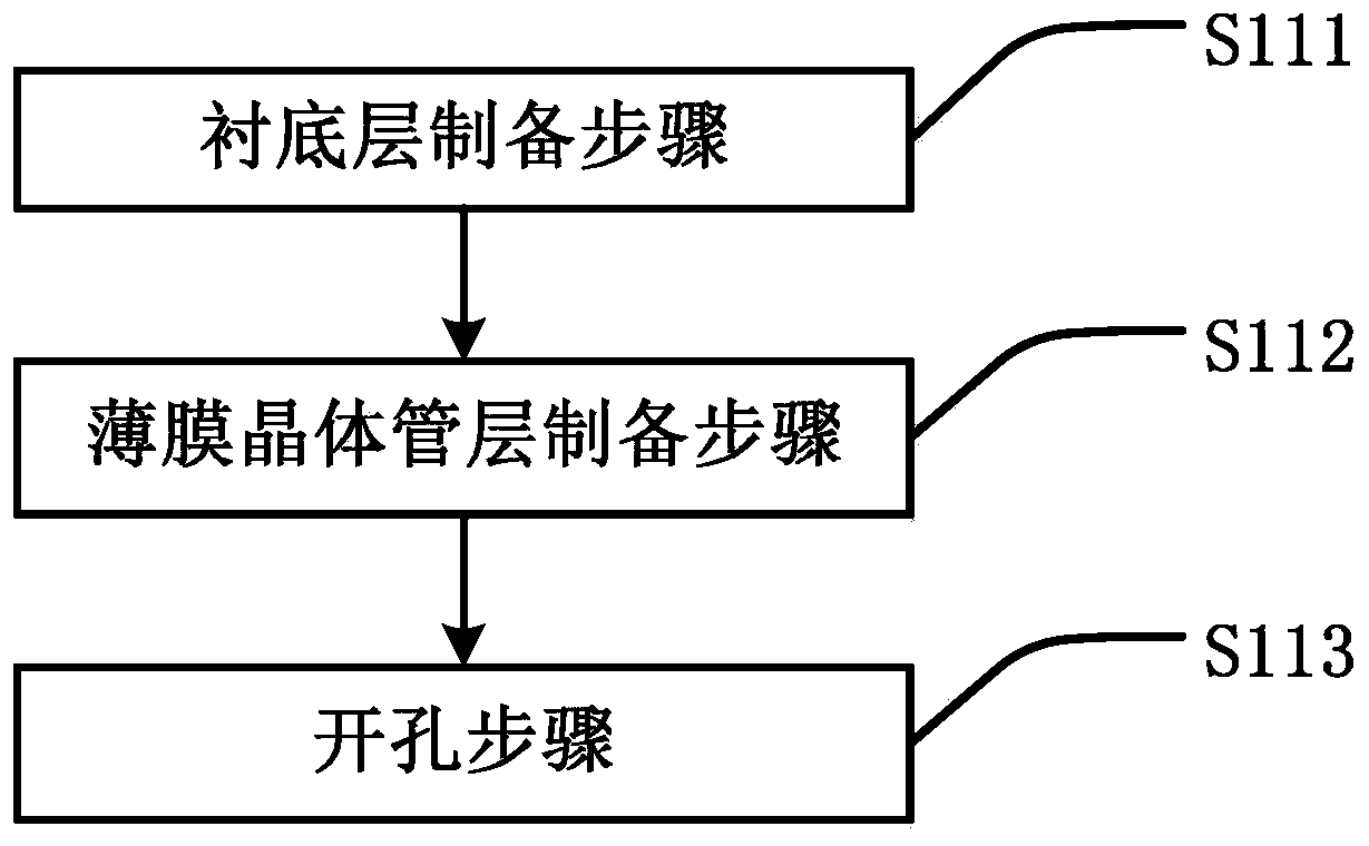
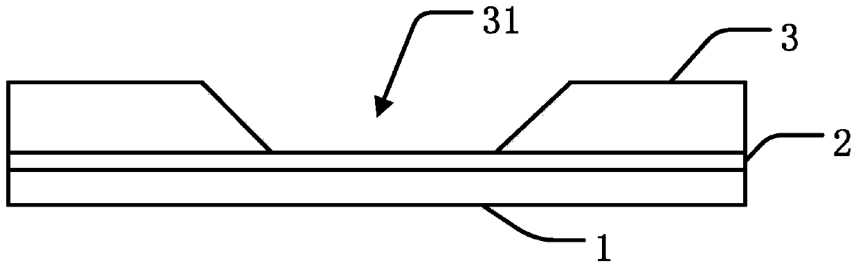
[0045] S101 substrate setting step, the substrate setting step includes steps S111~S113 (see figure 2 ), S111 substrate layer preparation step, prepare a substrate layer 2 on the upper surface of the substrate 1, the substrate layer 2 is made of polyimide (PI) or other buffer material, which plays the role of buffer protection. S112 TFT layer preparation step, preparing a TFT layer 3 on the upper surface of the substrate layer 2 . S113 opening step, opening holes downward on the upper surface of the thin film transistor layer 3 to form a through hole 31 (see image 3 ), the inner diameter of the through hole 31 gradually decreases from top to bottom, presenting a platform-shaped through hole structure.

[0046] S102 photoresist preparation step, preparing a photoresist 4 in the through hole 31, the photoresist preparation step includes steps S121-S...

Embodiment 2

[0066] like Figure 11 As shown, this embodiment provides a method for manufacturing a display panel, including steps S201-S207.

[0067] S201 substrate setting step, the substrate setting step includes steps S211 to S213 (see Figure 12 ), S211 substrate layer preparation step, prepare substrate layer 2 on the upper surface of substrate 1, the material of substrate layer 2 is polyimide (PI) or other buffer material, play the effect of buffer protection. Step S212 of preparing a thin film transistor layer, preparing a thin film transistor layer 3 on the upper surface of the substrate layer 2 . S213 opening step, opening holes downward on the upper surface of the thin film transistor layer 3 to form through holes 31 (see image 3 ), the inner diameter of the through hole 31 gradually decreases from top to bottom, presenting a platform-shaped through hole structure.

[0068] S202 photoresist preparation step, preparing photoresist 4 in the through hole 31, the photoresist pre...


PUM

PropertyMeasurementUnit
thicknessaaaaaaaaaa
thicknessaaaaaaaaaa

Abstract

The invention provides a display panel and a fabrication method. The fabrication method of the display panel comprises the following steps of substrate arrangement, photoresist preparation, protectionlayer fabrication, first inorganic layer fabrication, organic layer fabrication and second inorganic layer fabrication and also comprises the step of photoresist removal before or after the first inorganic layer fabrication, and the step of photoresist removal is used for removing photoresist in a through hole and a negative electrode layer and the protection layer on the photoresist. The fabrication method has the technical effects that laser cutting is not needed, the technical problem of particle adhesion caused by laser cutting is prevented, moreover, a crack-prevention structure is not needed to be arranged, the screen-to-body ratio of the display panel is improved, the performance of water and oxygen blocking of the display panel is improved, the package effect of a package film layer is improved, and the service lifetime of the display panel is prolonged.

Description

technical field [0001] The invention relates to the display field, in particular to a display panel and a preparation method thereof. Background technique [0002] The basic structure of an Organic Light Emitting Diode (OLED) is a thin, transparent indium tin oxide (ITO) with semiconductor properties connected to an anode, plus another metal cathode to form a sandwich-like structure. The whole structural layer includes: hole transport layer (HTL), light emitting layer (EL) and electron transport layer (ETL). [0003] OLED has self-luminous characteristics, unlike TFE LCD which requires a backlight, so the visibility and brightness are very high, and the voltage requirement is low and the power saving efficiency is high, plus fast response, light weight, thin thickness, simple structure, and low cost And other characteristics, it is regarded as one of the most promising products in the 21st century. [0004] Since the organic material of the light-emitting layer is quite se...

Claims


Application Information

Patent Timeline
Patent Type & Authority Applications(China)
IPC IPC(8): H01L51/56H01L51/52H01L27/32
CPCH10K59/12H10K50/844H10K59/1201H10K71/00
Inventor 彭斯敏金江江
Owner WUHAN CHINA STAR OPTOELECTRONICS SEMICON DISPLAY TECH CO LTD
Why Eureka
Try Eureka