Contact linear concentration sensor based on array waveguide grating structure and fluid detecting method thereof
A technology of arrayed waveguide grating and concentration sensor, which is applied in the direction of phase influence characteristic measurement, instrument, measurement device, etc., can solve problems such as being unfavorable for real-time sensing, and achieve the effect of accurate results
- Summary
- Abstract
- Description
- Claims
- Application Information
AI Technical Summary
Problems solved by technology
Method used
Image
Examples
Embodiment 1
[0045] A contact-type linear concentration sensor based on an arrayed waveguide grating structure, such as figure 2 and image 3 As shown, it includes a broadband optical signal input module 11, an arrayed waveguide grating, and a spectral signal detection module 12 connected in sequence; the broadband optical signal input module 11 integrates a broadband halogen fiber optic illuminator to provide a broadband light source; the arrayed waveguide grating It is used to correspond the change of fluid concentration to the drift of its own central wavelength; the spectral signal detection module 12 integrates a small CCD spectrometer inside, which is used to detect the drift of the output spectrum of the arrayed waveguide grating;
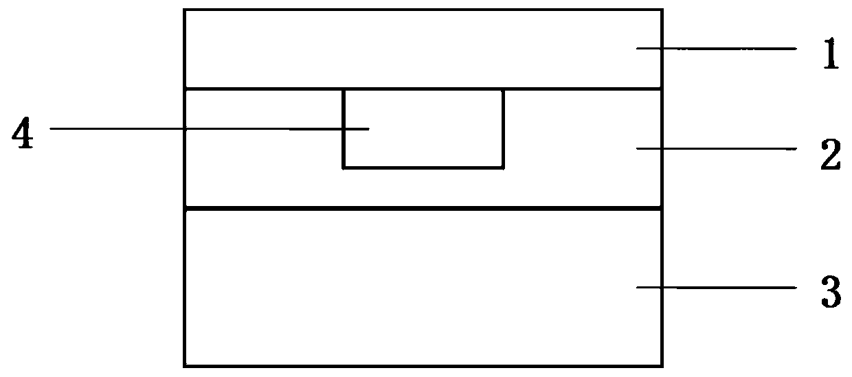
[0046] The single-mode waveguide includes a substrate 3 , a lower confinement layer 2 , a waveguide core layer 4 and an upper confinement layer 1 sequentially from bottom to top. The arrayed waveguide grating includes sequentially connected input chann...
Embodiment 2
[0051] A kind of contact type linear concentration sensor based on the arrayed waveguide grating structure described in embodiment 1, such as figure 1 As shown, the difference is that the structural size of the waveguide core layer 4 is designed to form a single-mode waveguide. The upper confinement layer 1 is the fluid-filled layer to be tested.
[0052] The material of the substrate 3 is silicon, silicon dioxide or polymethyl methacrylate.
[0053] Materials such as silicon, silicon dioxide, and polymethyl methacrylate have stable physical and chemical properties, and the preparation process is relatively mature, all of which are feasible choices for the preparation of optical waveguide devices.
[0054] The single-mode waveguide structure is a strip waveguide or a ridge waveguide, the width of the core layer of the single-mode waveguide is 0.5 μm-8 μm, and the thickness of the core layer of the single-mode waveguide is 0.5 μm-8 μm.
Embodiment 3
[0056] According to the contact linear concentration sensor based on the arrayed waveguide grating structure described in Embodiment 2, the difference is that the width of the core layer of the single-mode waveguide is 2 μm, and the thickness of the core layer of the single-mode waveguide is 1 μm.
PUM
| Property | Measurement | Unit |
|---|---|---|
| width | aaaaa | aaaaa |
| thickness | aaaaa | aaaaa |
| width | aaaaa | aaaaa |
Abstract
Description
Claims
Application Information
 - R&D Engineer
- R&D Manager
- IP Professional
- Industry Leading Data Capabilities
- Powerful AI technology
- Patent DNA Extraction
Browse by: Latest US Patents, China's latest patents, Technical Efficacy Thesaurus, Application Domain, Technology Topic, Popular Technical Reports.
© 2024 PatSnap. All rights reserved.Legal|Privacy policy|Modern Slavery Act Transparency Statement|Sitemap|About US| Contact US: help@patsnap.com


