Three-dimensional double-sided silicon micro-strip detector and preparation method thereof

A detector and double-sided technology, which is applied in the field of three-dimensional double-sided silicon microstripe detector and its preparation, can solve the problem that high-position resolution detectors are easily broken down, detector sensitivity is limited, and single-sided etching dead zone It can reduce the risk of breakdown, distribute the internal electric field uniformly, and simplify the electronics.

Pending Publication Date: 2019-07-12
XIANGTAN UNIV
View PDF0 Cites 2 Cited by
  • Summary
  • Abstract
  • Description
  • Claims
  • Application Information

AI Technical Summary

Problems solved by technology

[0005] In order to achieve the above purpose, the present invention provides a three-dimensional double-sided silicon microstrip detector and its preparation method, which solves the problem that the three-dimensional trench electrode detector in the prior art

Method used


Image

  • Three-dimensional double-sided silicon micro-strip detector and preparation method thereof
  • Three-dimensional double-sided silicon micro-strip detector and preparation method thereof
  • Three-dimensional double-sided silicon micro-strip detector and preparation method thereof

Examples


Embodiment 1

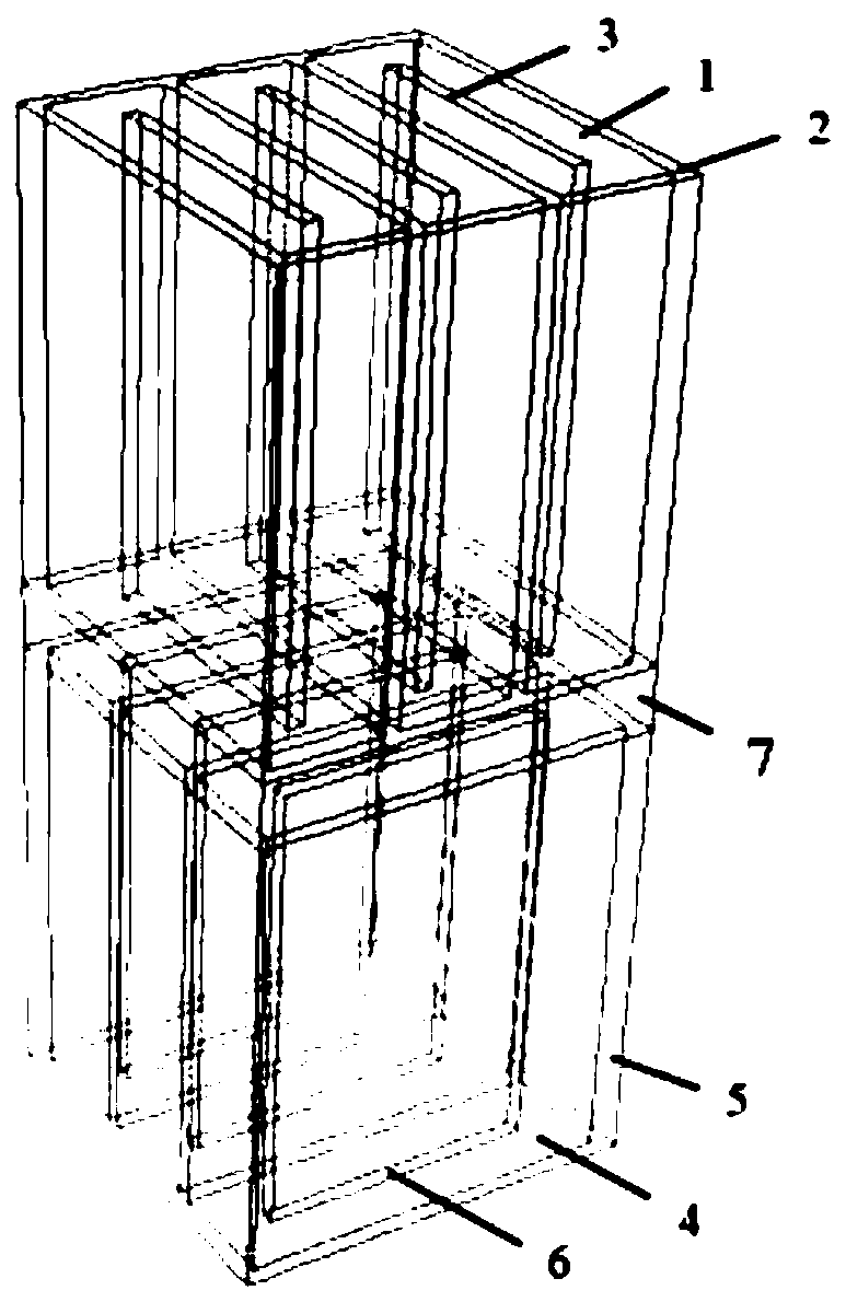
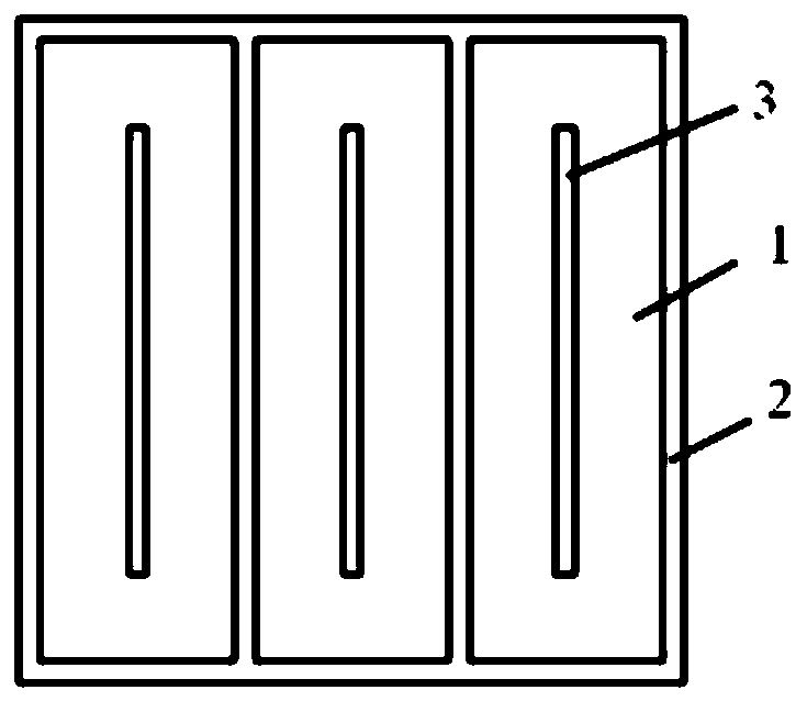
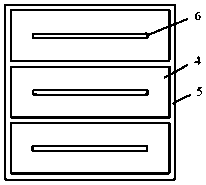
[0032] 3D double-sided silicon microstrip detectors, such as Figure 1~3 As shown, it includes an upper detection unit, a lower detection unit and an intermediate semiconductor substrate 7; the upper detection unit is etched on the upper part of the intermediate semiconductor substrate 7, the lower detection unit is etched on the lower part of the intermediate semiconductor substrate 7, and the upper detection unit is composed of the upper semiconductor substrate 1. The upper groove electrode 2 and the upper central electrode 3 are composed. The upper groove electrode 2 is a cuboid, and a plurality of parallel upper semiconductor substrates 1 are uniformly embedded in it. The upper semiconductor substrate 1 is embedded with an upper central electrode 3. The electrode interval between the trench electrode 2 and the upper central electrode 3 is r t , that is, the distance between the upper trench electrode 2 and the upper central electrode 3 is r t (The upper groove electrode 2...

Embodiment 2

[0034] The difference from Example 1 is that the doping concentration of the upper trench electrode 2 and the lower trench electrode 5 in this embodiment is 25×10 18 cm -3 The p-type heavily doped silicon substrate; the upper central electrode 3 and the lower central electrode 6 have a doping concentration of 25×10 18 cm -3 n-type heavily doped silicon substrate.

Embodiment 3

[0036] The difference from Examples 1-2 is that the doping concentration of the upper trench electrode 2 and the lower trench electrode 5 in this embodiment is 5×10 19 cm -3 The p-type heavily doped silicon substrate; the upper central electrode 3 and the lower central electrode 6 have a doping concentration of 5×10 19 cm -3 n-type heavily doped silicon substrate.


PUM

PropertyMeasurementUnit
Doping concentrationaaaaaaaaaa

Abstract

The invention discloses a three-dimensional double-sided silicon micro-strip detector and a preparation method thereof. The three-dimensional double-sided silicon micro-strip detector comprises an upper portion detection unit, a lower portion detection unit and a middle semiconductor base body, a plurality of mutually parallel upper semiconductor base bodies are uniformly inlaid in an upper troughelectrode of the upper portion detection unit, and upper central electrodes are inlaid in the upper semiconductor base bodies; a plurality of mutually parallel lower silicon base bodies are uniformlyinlaid into the lower trough electrode of the lower portion detection unit, and lower central electrodes are inlaid in the lower silicon base bodies; the heights of the upper semiconductor base bodies, the upper trough electrodes, the upper central electrodes, the lower silicon base bodies, the lower trough electrodes and the lower central electrodes are the same; the lower portion detection unitis located below the upper portion detection unit, and the lower portion detection unit and the upper portion detection unit are staggered for a certain angle in a horizontal direction. A silicon dioxide layer is generated at the surface of a silicon wafer by employing the gettering oxidation technology, the detector pattern is transferred onto the silicon dioxide layer through marking and photoetching, the etching and chemical deposition diffusion of the cathode electrode and the anode electrode are performed, and finally, damaging repairing and package are performed.

Description

technical field [0001] The invention belongs to the technical field of photon (including X-ray, laser, X-ray free electron laser) or particle detection, and relates to a three-dimensional double-sided silicon microstrip detector and a preparation method thereof. Background technique [0002] Detectors are mainly used in high-energy physics, astrophysics, aerospace, military, medical technology and other fields. When using silicon microstrip detectors and silicon pixel detectors to measure the position resolution of particles, there are the following deficiencies: the two detection The depletion direction of the detector is from the upper surface of the chip to the lower surface of the chip, and the depletion width is equal to the thickness of the chip (generally 300 microns), which makes the depletion voltage of the two-dimensional detector very high. The higher the irradiation, the higher the power consumption and easy to break down. Therefore, although the silicon microstr...

Claims


Application Information

Patent Timeline
IPC IPC(8): H01L25/04H01L31/0224H01L31/08H01L31/18
CPCH01L25/041H01L31/0224H01L31/085H01L31/18Y02P70/50
Inventor 李正张亚
Owner XIANGTAN UNIV
Why Eureka
Try Eureka