Device and process for glue removal of large-size round-bar silicon single crystal subjected to multi-wire cutting
A multi-wire cutting, silicon single crystal technology, used in fine working devices, manufacturing tools, stone processing equipment, etc., can solve the problems of sticking to the surface of silicon wafers, potential safety hazards, harsh environment, etc., and reduce edge chipping and splintering. production, simplified process, and the effect of improving the filming rate
Inactive Publication Date: 2019-06-28
GRINM SEMICONDUCTOR MATERIALS CO LTD
View PDF6 Cites 1 Cited by
- Summary
- Abstract
- Description
- Claims
- Application Information
AI Technical Summary
Problems solved by technology
[0004] The purpose of the present invention is to provide a new degumming device and process for the PEG suspension in the middle part of the large-size silicon wafer, which is easy to oxidize and stick to the surface of the silicon wafer in hot water, and the hot water degumming exists in the harsh environment and potential safety hazards.
Method used
View moreImage
Smart ImageViewing Examples

Examples
Embodiment 1
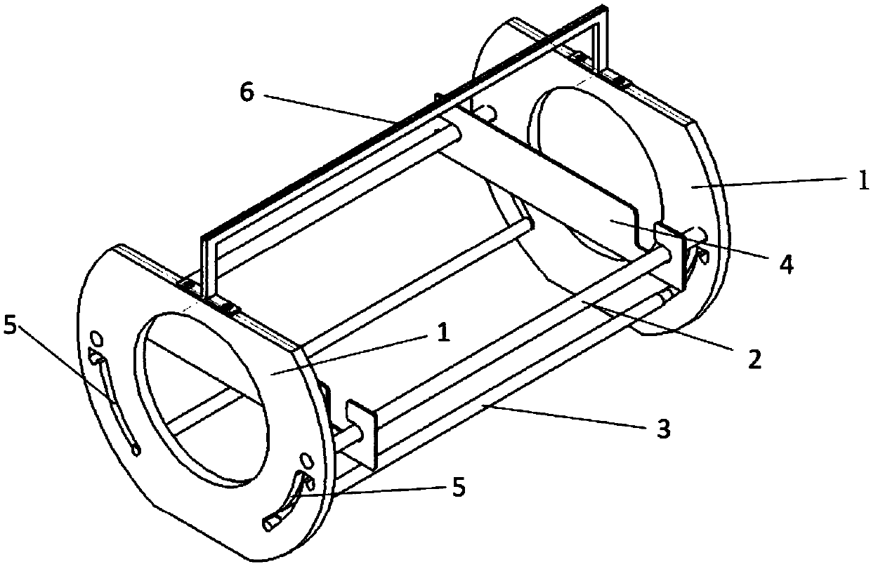
[0029] Adjust the position of the arc-shaped chute in the device according to the size of the 8-inch wafer to achieve relative fixation of the wafer and the device.
Login to View More PUM
 Abstract
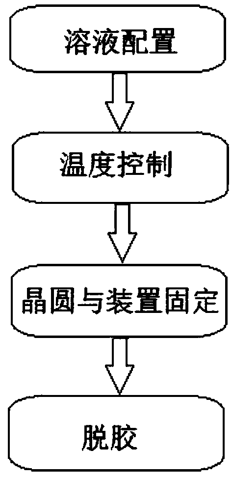
The invention discloses a device and a process for glue removal of a large-size round-bar silicon single crystal subjected to multi-wire cutting. The device comprises two fixing plates, two supportingrods, two sliding rods and two detachable inserting sheets; the two fixing plates are fixed and supported through the two supporting rods, two arc-shaped sliding grooves are symmetrically formed in each fixing plate, the sizes of the circles where the two arc-shaped sliding grooves in the same fixing plate are located are equivalent to the size of a wafer, the two sliding rods are arranged between the two fixing plates in parallel, the end parts of the two sliding rods are located in the arc-shaped sliding grooves, and the two sliding rods can slide along the arc-shaped sliding grooves; and the inserting sheets at the two ends are used for axially positioning the silicon wafer and carrying out axial adjustment according to the length of a crystal rod. The process comprises the following steps of (1) preparing a solution; (2) controlling the temperature of the solution; (3) fixing the wafer to the device; and (4) glue removal and the like. The device and the process can play a role inpre-cleaning the surface of the wafer, the processes of manual glue removal is further simplified, generation of edge breakage and wafer cracking in the glue removal process is reduced, and the yieldof the single crystal slicing is improved.
Description
technical field [0001] The invention relates to a device and process for degumming after multi-wire cutting of large-size round silicon single crystal. Background technique [0002] The glue used before single crystal cutting is generally boiled glue, which can be softened in hot water, and the glue and silicon wafers are separated by using the different thermal expansion ratios of the glue and silicon wafers, but there are always the following disadvantages : The degumming time is long, and the silicon wafer is easily oxidized; the center of the silicon wafer is difficult to penetrate due to the degumming agent, and the PEG solution used for cutting works together with the oxide film on the surface of the silicon wafer in hot water, so it is difficult to adsorb on the surface of the silicon wafer. Carry out follow-up cleaning; In addition, this method requires the operator's hands to be in contact with hot water, which has certain potential safety hazards. Therefore, the m...
Claims
Login to View More Application Information
Patent Timeline
 Patent Type & Authority Applications(China)
IPC IPC(8): B28D5/00
Inventor 苏冰安瑞阳王新曲翔史训达
Owner GRINM SEMICONDUCTOR MATERIALS CO LTD
Features
- R&D
- Intellectual Property
- Life Sciences
- Materials
- Tech Scout
- Unparalleled Data Quality
- Higher Quality Content
- 60% Fewer Hallucinations
Learn More Browse by: Latest US Patents, China's latest patents, Technical Efficacy Thesaurus, Application Domain, Technology Topic, Popular Technical Reports.
© 2025 PatSnap. All rights reserved.Legal|Privacy policy|Modern Slavery Act Transparency Statement|Sitemap|About US| Contact US: help@patsnap.com