Micron full-color qled array device and its preparation method based on deep silicon etching template quantum dot transfer process
A deep silicon etching, quantum dot technology, applied in semiconductor devices, electric solid devices, electrical components and other directions, can solve the problems of complex process, difficult to achieve multi-color quantum dot filling and transfer, etc., to achieve color conversion, low cost , Spin coating with high quality effect
- Summary
- Abstract
- Description
- Claims
- Application Information
AI Technical Summary
Problems solved by technology
Method used
Image
Examples
Embodiment 1
[0084] Example 1 Micron full-color QLED array device based on deep silicon etching template quantum dot transfer process
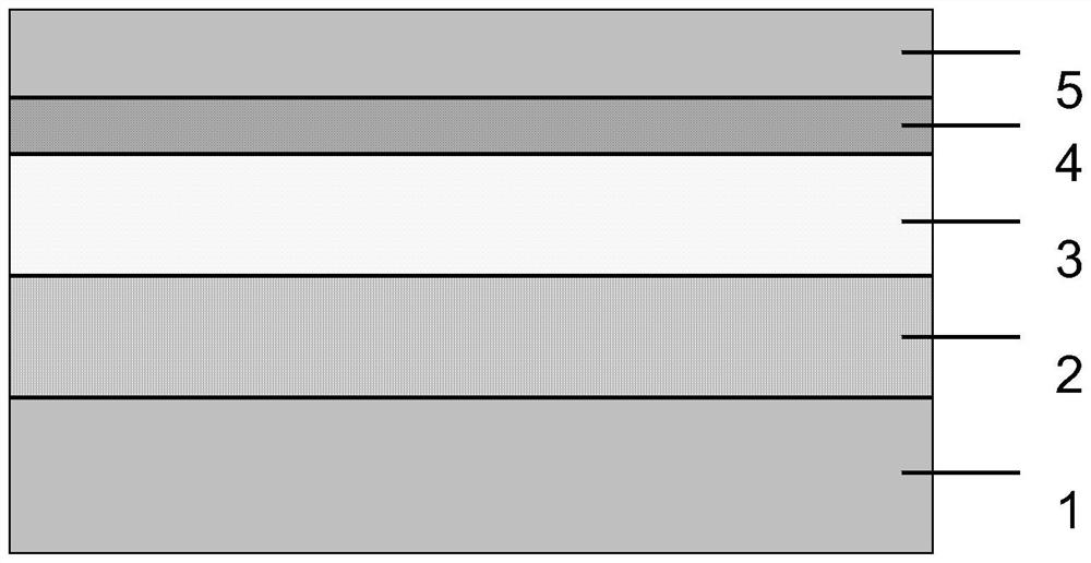
[0085] The epitaxial wafer structure selected for the substrate material in this implementation case is as follows figure 1 As shown, a standard blue LED epitaxial wafer with a p-n structure includes a sapphire substrate 1; a gallium nitride buffer layer 2 grown on the sapphire substrate; an n-type gallium nitride layer 3 grown on the buffer layer; A quantum well active layer 4 on the quantum well active layer; a p-type gallium nitride layer 5 grown on the quantum well active layer.
[0086] The specific preparation method of the Micro-LED array device is as follows:
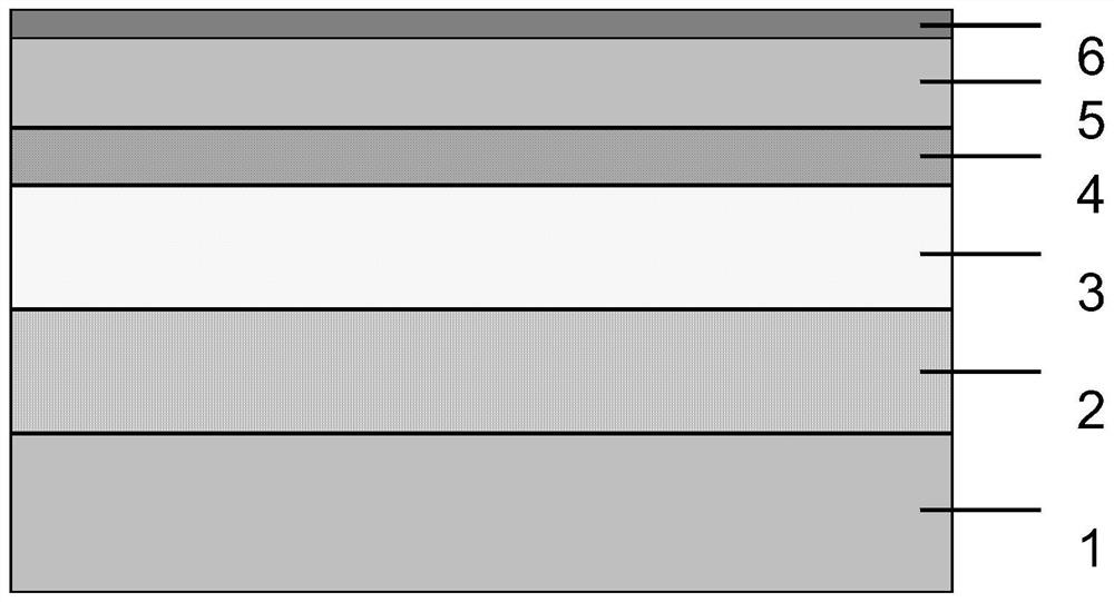
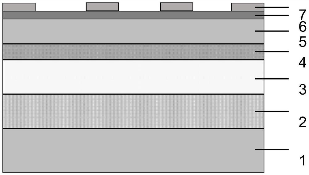
[0087] (1) if figure 2 As shown, using plasma-enhanced chemical vapor deposition (PECVD) technology, in In x Ga 1-x Evaporation of a layer of 150nm thick SiO on N / GaN quantum well blue LED epitaxial wafer 2 Dielectric layer 6, PECVD grown SiO 2 The way is to pass 5% SiH into the react...
Embodiment 2
[0108] Example 2 Micron full-color QLED array device based on deep silicon etching template quantum dot transfer process
[0109] The epitaxial wafer structure selected for the substrate material in this implementation case is as follows figure 1 As shown, a standard blue LED epitaxial wafer with a p-n structure includes a sapphire substrate 1; a gallium nitride buffer layer 2 grown on the sapphire substrate; an n-type gallium nitride layer 3 grown on the buffer layer; A quantum well active layer 4 on the quantum well active layer; a p-type gallium nitride layer 5 grown on the quantum well active layer.
[0110] The specific preparation method of the Micro-LED array device is as follows:
[0111] (1) if figure 2 As shown, using plasma-enhanced chemical vapor deposition (PECVD) technology, in In x Ga 1-x Evaporation of a layer of 200nm thick SiO on N / GaN quantum well blue LED epitaxial wafer 2 Dielectric layer 6, PECVD grown SiO 2 The way is to pass 5% SiH into the react...
Embodiment 3
[0132] Example 3 Micron full-color QLED array device based on deep silicon etching template quantum dot transfer process
[0133] The epitaxial wafer structure selected for the substrate material in this implementation case is as follows figure 1 As shown, a standard blue LED epitaxial wafer with a p-n structure includes a sapphire substrate 1; a gallium nitride buffer layer 2 grown on the sapphire substrate; an n-type gallium nitride layer 3 grown on the buffer layer; A quantum well active layer 4 on the quantum well active layer; a p-type gallium nitride layer 5 grown on the quantum well active layer.
[0134] The specific preparation method of the Micro-LED array device is as follows:
[0135] (1) if figure 2 As shown, using plasma-enhanced chemical vapor deposition (PECVD) technology, in In x Ga 1-x Evaporation of a layer of 250nm thick SiO on N / GaN quantum well blue LED epitaxial wafer 2 Dielectric layer 6, PECVD grown SiO 2 The way is to pass 5% SiH into the react...
PUM
| Property | Measurement | Unit |
|---|---|---|
| thickness | aaaaa | aaaaa |
| thickness | aaaaa | aaaaa |
| thickness | aaaaa | aaaaa |
Abstract
Description
Claims
Application Information
 - R&D
- Intellectual Property
- Life Sciences
- Materials
- Tech Scout
- Unparalleled Data Quality
- Higher Quality Content
- 60% Fewer Hallucinations
Browse by: Latest US Patents, China's latest patents, Technical Efficacy Thesaurus, Application Domain, Technology Topic, Popular Technical Reports.
© 2025 PatSnap. All rights reserved.Legal|Privacy policy|Modern Slavery Act Transparency Statement|Sitemap|About US| Contact US: help@patsnap.com


