Inverted T Tunneling Field Effect Transistor

A technology of tunneling field effect and transistor, which is applied in the direction of semiconductor devices, electrical components, circuits, etc., can solve the problems of low tunneling efficiency, low on-state current, large static power consumption of devices, etc., and achieve good gate control ability, Effect of Low Subthreshold Swing

Inactive Publication Date: 2020-07-14
NORTHWESTERN POLYTECHNICAL UNIV
View PDF4 Cites 0 Cited by
  • Summary
  • Abstract
  • Description
  • Claims
  • Application Information

AI Technical Summary

Problems solved by technology

However, the band tunneling efficiency of ordinary tunneling field effect transistors is low, so that the on-state current of ordinary tunneling transistors is lower than that of traditional field effect transistors, and the gate voltage of tunneling transistors can be both forward and reverse biased. Generates a considerable amount of tunneling current, which makes the device have a large static power consumption
It is difficult to meet the device requirements of large-scale integrated systems, so a new type of structural device is required to maintain a steep sub-threshold swing while significantly reducing static power consumption and increasing the forward on-state current when the transistor is turned on

Method used


Image

  • Inverted T Tunneling Field Effect Transistor
  • Inverted T Tunneling Field Effect Transistor
  • Inverted T Tunneling Field Effect Transistor

Examples


Embodiment Construction

[0028] The present invention will be further described below in conjunction with the drawings and embodiments.

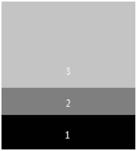
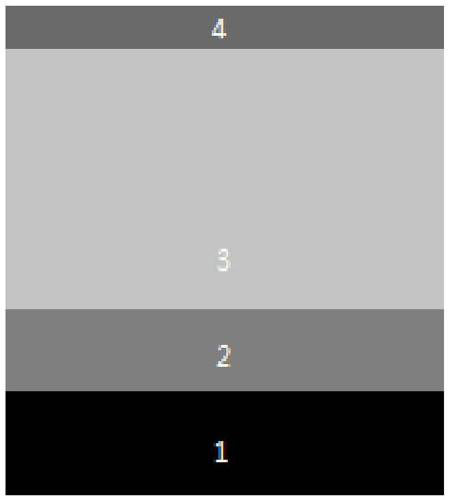
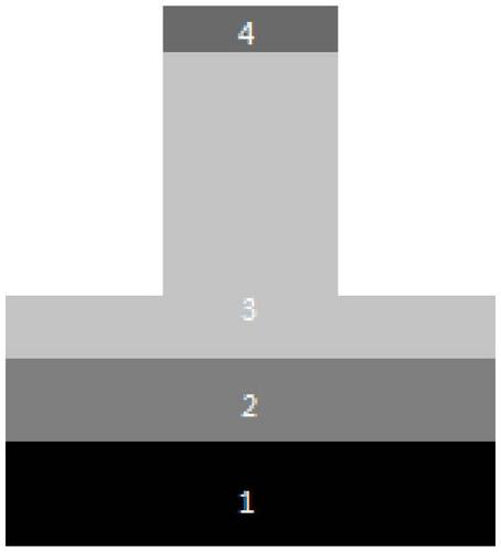
[0029] An inverted T tunneling field effect transistor, including the silicon substrate of the SOI wafer, the silicon substrate of the SOI wafer is the substrate insulating layer of the SOI wafer, and the substrate insulating layer of the SOI wafer is heavily doped Miscellaneous source region, two monocrystalline silicon films, and two heavily doped drain regions. The heavily doped source region is located in the middle above the insulating layer of the substrate. The two monocrystalline silicon films are both L-type and are located at the heavily doped source. The two heavily doped drain regions are located on the L-shaped bottom of the monocrystalline silicon film and are close to the outer edge of the lateral edge of the substrate insulating layer of the SOI wafer, and are located in the substrate insulating layer. Above; the two monocrystalline silicon film L-shape...


PUM

PropertyMeasurementUnit
thicknessaaaaaaaaaa

Abstract

The invention provides an inverted T-shaped tunneling field effect transistor. A substrate insulating layer of an SOI wafer is arranged above a silicon substrate of the SOI wafer; a heavily-doped source region, two monocrystalline silicon thin films and two heavily-doped drain regions are arranged above the substrate insulating layer of the SOI wafer; gate insulating layers are arranged on the twosides of the L shape of the two monocrystalline silicon thin films respectively; the two sides of each gate insulating layer are provided with insulating medium barrier layers respectively; gates arearranged on the two sides of each gate insulating layer, and above the insulating medium barrier layers; the two gates are positioned on the insulating medium barrier layers on the two sides respectively and are in contact with the gate insulating layers on the two sides respectively; gate electrodes are located above the gates; source electrodes are located above the heavily-doped source region;and drain electrodes are located above the heavily-doped drain regions. The inverted T-shaped tunneling field effect transistor has good gate control capability, and has excellent sub-threshold characteristics and forward conduction capability, so that a device has good low reverse leakage current and static power consumption while the forward characteristics are ensured.

Description

Technical field [0001] The invention relates to the field of semiconductor technology, in particular to a tunneling field effect transistor with low power consumption. Background technique [0002] With the development of ultra-large-scale integrated circuits, the size of traditional semiconductor devices has become smaller and smaller. However, it has not only increased the difficulty of production process, but also various adverse effects have become more and more obvious. When the size of semiconductor devices enters the nanometer era, due to their own physical characteristics, their sub-threshold swing cannot always exceed the 60mV / dec limit, and there are also problems such as excessive reverse leakage current. In response to these problems, researchers have now proposed a more effective method to solve the sub-threshold swing and other issues, using a new type of device tunneling field effect transistor to replace the traditional field effect transistor, reducing the tradit...

Claims


Application Information

Patent Timeline
Patent Type & Authority Patents(China)
IPC IPC(8): H01L29/06H01L29/417H01L29/423H01L29/739
Inventor 韩茹张海潮王党辉安建峰黄小平张萌陈超
Owner NORTHWESTERN POLYTECHNICAL UNIV
Why Eureka
Try Eureka