A millimeter wave variable gain amplifier structure

A gain amplifier, millimeter-wave technology, applied in differential amplifiers, DC-coupled DC amplifiers, gain control, etc., can solve the problem of high cost, power and integration compromise, and difficult to meet the high gain adjustment range of millimeter-wave phased arrays Low precision phase shift and other issues, to achieve the effect of reducing phase shift, good linearity and stability, and improving gain adjustment range and accuracy

Active Publication Date: 2019-05-21
CLIVIA SEMICON TECH CO LTD
View PDF15 Cites 5 Cited by
  • Summary
  • Abstract
  • Description
  • Claims
  • Application Information

AI Technical Summary

Problems solved by technology

The main challenges faced by 5G millimeter-wave phased array MMIC chips include the compromise of power and integration, precise control of phase and amplitude, efficiency under advanced working conditions, and in-band and out-of-band non-ideal effects under high bandwidth.
Therefore, the traditional variable gain amplifier structure and attenuator are difficult to meet the requirements of high gain adjustment range, high precision and low phase shift in millimeter wave phased array applications
Variable gain amplifiers, whose circuits generally use high-electron mobility transistor (high-electron mobility transistor, HEMT) monolithic-microwave-integrated-circuit (monolithic-microwave-integrated-circuit) technology, such as gallium nitride (GaN) and gallium arsenide (GaAs) processes, but they are relatively expensive

Method used


Image

  • A millimeter wave variable gain amplifier structure
  • A millimeter wave variable gain amplifier structure
  • A millimeter wave variable gain amplifier structure

Examples


Embodiment 1

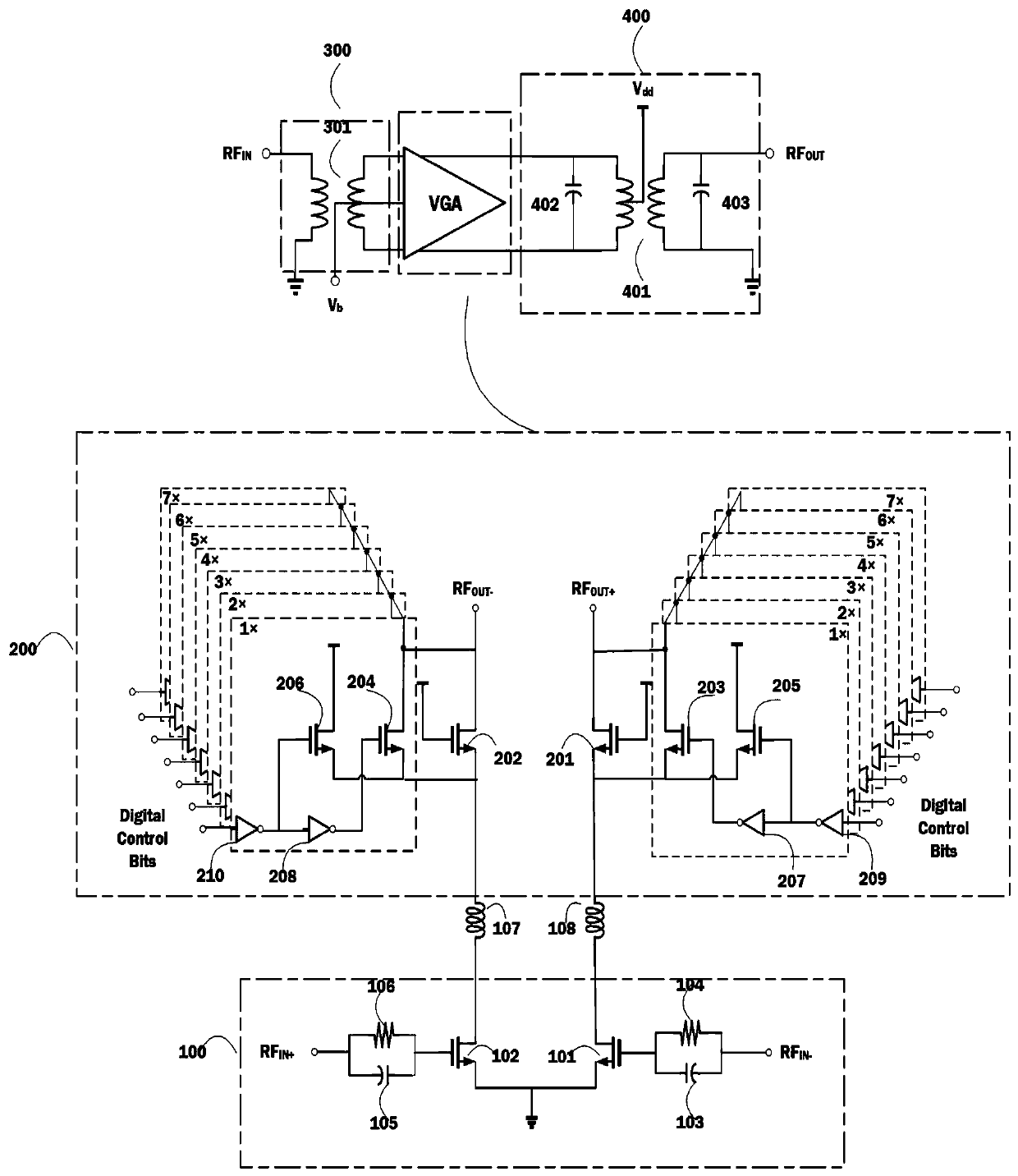
[0031] Such as Figure 1A As shown, a millimeter-wave variable gain amplifier structure, including a first part of the circuit 100 composed of common source transistors; a second part of the circuit 200 that generates a variable gain output signal; a third part of the circuit 300 composed of an input matching network ; by the fourth part of the circuit 400 of the output matching network.

[0032] The first part of the circuit 100 composed of common source transistors of the present invention is composed of two N-type field effect transistors 101 and 102 . The sources of the two N-type field effect transistors 101 and 102 are coupled to ground to form a common-source differential pair, and their gates are respectively connected to the input voltage RF IN+ ,RF IN- . In addition, the first interstage inductance 107 is connected in series with the source of the first common gate transistor 201 and the drain of the first common source transistor 101, and the second interstage ind...


PUM


Abstract

The invention discloses a millimeter wave variable gain amplifier structure, and relates to the technical field of electronic circuit design, in particular to the technical field of radio frequency variable gain amplifier design suitable for a millimeter wave phased array system. The circuit comprises a first part of circuit formed by a common source transistor; A second partial circuit that generates a variable gain output signal; A third part circuit composed of an input matching network; And a fourth part of circuit of the output matching network. According to the invention, the purposes oflow cost, suitability for CMOS technology, high gain, large adjustment range, high precision and low phase shift are achieved.

Description

technical field [0001] The invention relates to the technical field of electronic circuit design, in particular to the technical field applicable to the design of radio frequency variable gain amplifiers in millimeter wave phased array systems. Background technique [0002] With the development of 5G communication technology, the millimeter wave phased array system has become a research hotspot because of its unique advantages. Compared with 4G, the transmission distance of millimeter wave signals is shorter. Due to factors such as shorter wavelengths and air absorption, the transmission distance of 5G signals is about 200 meters. In order to meet the data traffic demand of short-distance transmission range, 5G will adopt massive multiple-input multiple-output technology (Massive MIMO) to double the system communication capacity by using multiple antennas. In addition to the reference in 5G communication technology, the application of millimeter wave technology in the mil...

Claims


Application Information

Patent Timeline
Patent Type & Authority Applications(China)
IPC IPC(8): H03G3/30H03F3/45
Inventor 柴远
Owner CLIVIA SEMICON TECH CO LTD
Why Eureka
Try Eureka