
Method for adjusting surface energy level and energy band of semiconductor material

A surface energy level and semiconductor technology, which is applied in the manufacture of semiconductor/solid-state devices, discharge tubes, electrical components, etc., can solve the problems of inconsistency in characteristic parameters and weak regulation, and achieve reduced energy consumption, low energy consumption, and no macroscopic The effect of temperature rise

Active Publication Date: 2019-05-21
UNIV OF ELECTRONICS SCI & TECH OF CHINA
View PDF2 Cites 1 Cited by
  • Summary
  • Abstract
  • Description
  • Claims
  • Application Information

AI Technical Summary

Problems solved by technology

[0005] The purpose of the present invention is to propose a method for regulating the surface energy level and energy band of semiconductor materials in view of the problems that the characteristic parameters of semiconductor materials in other regulation methods cannot be taken into account, the regulation is relatively small, and the problems of impurity introduction are brought about in the background technology. method

Method used


Image

  • Method for adjusting surface energy level and energy band of semiconductor material
  • Method for adjusting surface energy level and energy band of semiconductor material
  • Method for adjusting surface energy level and energy band of semiconductor material

Examples


Embodiment 1

[0027] A method for regulating the surface energy level of an FTO semiconductor material, comprising the following steps:

[0028] Step 1. Select the fluorine-doped tin oxide semiconductor (FTO) material on the glass substrate, place it in acetone, absolute ethanol and water for ultrasonic cleaning, each time for 10 minutes, and dry it for later use after ultrasonic;

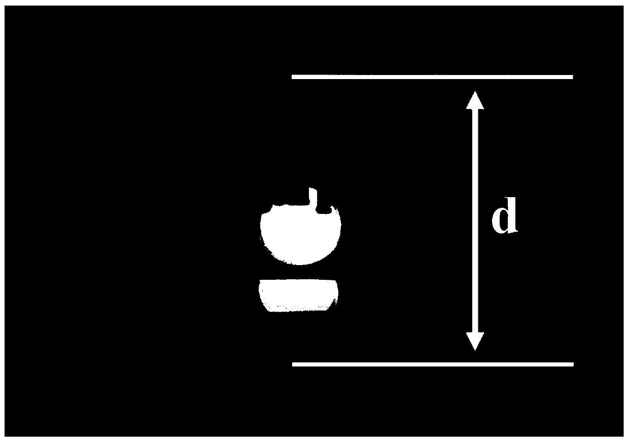
[0029] Step 2. Place the glass substrate with FTO semiconductor material cleaned in step 1 on the metal lower plate in the chamber of the plasma processing instrument. The distance between the two metal plates is 34mm, and the upper plate is connected to a 27MHz radio frequency Power supply, the lower plate is connected to a 13.56MHz radio frequency power supply, wherein the plate spacing can change the position of the plasma sheath, so that the surface of the FTO is in the plasma sheath, the upper plate generates plasma, and the lower plate provides additional bias for the plasma, so that increased plasma bomba...

Embodiment 2

[0035] Process the FTO according to the steps in Example 1, only adjust the discharge power of the upper plate in step 4 to 50W, 100W, 180W, and keep other steps unchanged. The resistive light transmission and reflection of the processed FTO obtained in this embodiment are as follows: figure 2 Shown; X-ray diffraction pattern (XRD) spectrum and X-ray photoelectron spectrum (XPS) are as image 3 shown.

Embodiment 3

[0037] A method for regulating the surface energy level of an FTO semiconductor material, comprising the following steps:

[0038] Step 1. Select the fluorine-doped tin oxide semiconductor material on the glass substrate, place it in acetone, absolute ethanol and water for ultrasonic cleaning, each time for 10 minutes, and dry it for later use after ultrasonic;

[0039] Step 2. Place the glass substrate with FTO semiconductor material cleaned in step 1 on the metal lower plate in the chamber of the plasma processing instrument. The distance between the two metal plates is 34mm, and the upper plate is connected to a 27MHz radio frequency Power supply, the lower plate is connected to a 13.56MHz RF power supply;

[0040] Step 3. Vacuumize the chamber of the plasma processor to keep the background vacuum degree less than 10 -3 Pa; then fill the vacuum chamber with argon with a purity of 99.999% and O with a purity of 99.99% 3, the flow rate ratio of argon and ozone is 3:1, so th...


PUM


Abstract

The invention provides a method for adjusting surface energy level and energy band of a semiconductor material, and belongs to the technical field of the semiconductor material. The method provided bythe invention is based on oxygen plasma processing, is capable of continuously controlling the surface chemical composition, the defect state density, the energy level and the energy band of the semiconductor material on premise of not affecting the light transmittance and the conductivity of the semiconductor material, and reduces the back recombination of the interface carrier. The plasma surface treatment technology designed by the invention uses the radio-frequency discharge as the plasma excitation method, uses the oxygen plasma to process the semiconductor material, selectively removesthe doped atoms of the surface of the material by utilizing the characteristics of the low macroscopic temperature and the high particle energy of the radio-frequency plasma and the extremely close atomic radius of the oxygen and the atomic radius of the semiconductor material, and prepares the semiconductor material with the continuously-adjustable surface energy level and energy band through optimizing the parameters of the power, the processing time, etc.

Description

technical field [0001] The invention belongs to the technical field of semiconductor materials, and in particular relates to a method for regulating the surface energy level and energy band of semiconductor materials. Background technique [0002] Semiconductor materials are widely used because of their unique semiconductor properties in light, heat, magnetism, electricity and other fields. Various semiconductor devices based on semiconductor materials are also used in all aspects of life. For example, TiO2 materials are used in the field of photocatalysis, GaAs materials are used in microelectronic devices, GaN is used in optoelectronic devices, etc. Although there are many kinds of semiconductor materials, they have some inherent characteristics, which are called characteristic parameters of semiconductor materials. Because different uses require different material characteristics, this parameter is very important for material applications. The characteristic parameters o...

Claims


Application Information

Patent Timeline
Patent Type & Authority Applications(China)
IPC IPC(8): H01L21/322H01J37/32
Inventor 熊杰孙浩轩晏超贻杜新川黄建文邬春阳戴丽萍
Owner UNIV OF ELECTRONICS SCI & TECH OF CHINA
Learn More