Eureka AIR delivers breakthrough ideas for toughest innovation challenges, trusted by R&D personnel around the world.

Polymer, display panel and display device

A technology of polymers and connection positions, which is applied in the direction of luminescent materials, chemical instruments and methods, and electric solid devices, etc., to achieve the effects of shortening the conjugate length, weakening charge transfer, and increasing energy levels

Active Publication Date: 2019-04-26
WUHAN TIANMA MICRO ELECTRONICS CO LTD
View PDF4 Cites 10 Cited by
  • Summary
  • Abstract
  • Description
  • Claims
  • Application Information

AI Technical Summary

Problems solved by technology

Although there are more and more reported carbazole polymer-based TADF materials, there are still few materials with high quantum efficiency.

Method used


Image

  • Polymer, display panel and display device
  • Polymer, display panel and display device
  • Polymer, display panel and display device

Examples


Embodiment 1

[0103] Synthesis of Polymer M1

[0104] The synthetic route of polymer M1 is shown below.

[0105]

[0106] The synthesis steps of polymer M1 are as follows:

[0107]

[0108] In a 200ml stuffy tank, sequentially add compound A (5.12, 20mmol), compound B (9.14g, 20mmol), anhydrous toluene 100ml and BBr 3 (10g, 40mmol), start stirring, heat up to 120°C and stir for 12h. After the reaction is over, slowly add 70ml of ice water to quench, then add dichloromethane (100ml×3) to extract the reaction solution, and then use saturated brine (100ml ×2) Washing, liquid separation, drying, filtration, spin-drying of the filtrate, and recrystallization using toluene / ethanol to obtain white solid C with a yield of 80%.

[0109] MALDI-TOF: 604.99

[0110] 1 H NMR(400MHz,C):δ7.81(s,3H),7.66(s,2H),7.36(s,3H),7.30(d,J=12.2Hz,2H),4.15(s,2H), 1.73(s,2H),1.29(d,J=27.9Hz,10H),0.89(s,3H).

[0111] 13 C NMR (100MHz, CDCl 3 ): δ167.29(s), 143.65(s), 140.34(s), 135.67(s), 134.81(s), 133.8...

Embodiment 2

[0123] The electroluminescent properties of the exemplary polymeric materials M1, M2, M3 and M4 described herein were simulated using Gaussian software.

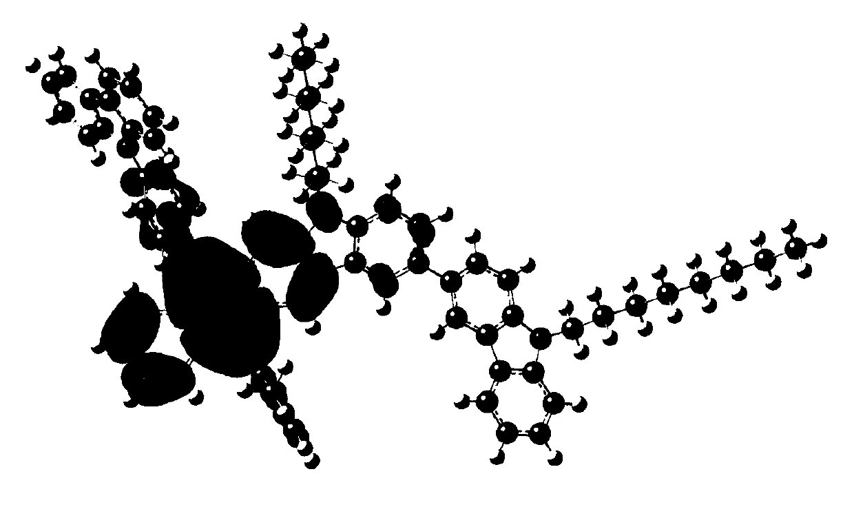
[0124] figure 2 with image 3 The HOMO and LUMO energy level diagrams of exemplary polymer M1 of the present invention are shown. It can be clearly seen from the figure that the HOMO and LUMO of the polymer molecule are respectively arranged on the donor unit and the acceptor unit, realizing the complete separation of HOMO and LUMO, which helps to reduce the intersystem energy difference ΔE ST , so as to improve the inverse intersystem crossing ability.

[0125] Table 1 Parameters of four representative polymers

[0126]

Embodiment 3

[0128] Taking M1 as an example, it is used as a fluorescent dopant (guest material), and the classic polymer material PVK is used as the host material, and the doped device structure is designed:

[0129] ITO (100 nm) / PEDOT:PSS (60 nm) / PVK:M1 (40 nm, 5%) / TmPyPb (50 nm) / LiF (0.5 nm) / Al (100 nm).

[0130] Similarly, the design comparison device structure is as follows:

[0131] ITO (100 nm) / PEDOT:PSS (60 nm) / PVK:BCzVBi (40 nm, 5%) / TmPyPb (50 nm) / LiF (0.5 nm) / Al (100 nm).

[0132] Fabrication of OLED devices

[0133] The structure of the OLED device is as Image 6 As shown, the brief description of its production process is as follows: put the substrate 1 into a rotary washing and drying machine, first wash it with deionized water and flush it with nitrogen, and then treat it with ultraviolet light for 20 minutes to completely remove the residual oil on the surface and improve the anode 2 (the material is ITO) work function, using a combination of high and low speed, two-way s...


PUM


Abstract

The invention belongs to the technical field of OLEDs (organic light emitting diodes) and provides a polymer of a structure of formula (I) as shown in the specification. In the formula, R1 and R2 arerespectively selected from C1-C20 alkyl, C3-C20 naphthenic base, C1-C20 alkoxyl and substituted or unsubstituted aryl or heteroaryl; L is selected from single bonds, phenyl, naphthyl, pyridyl, pyrimidyl and pyrazinyl; R3 is selected from substituted or unsubstituted aryl or heteroaryl; R4 is selected from alkyl or alkoxyl of C4-C20; n is greater than or equal to 4. The polymer provided by the invention comprises heterocyclic boron-carbazole structure and has TADF (thermal activation delay fluorescence) properties, when the polymer is used in an organic light emitting diode, light can be emitted from triplet exciton with transition inhibition of conventional fluorescence molecules, and thus the efficiency of a device can be improved. Meanwhile, a carbazole polymer type TADF material self has a bipolar property, when the polymer is used as a main body or secondary material of a light emitting layer, the transmission capability of two charge carriers and charge carrier balance can be greatly improved, the fluorescence quantum efficiency can be improved, and the voltage of the device can be reduced.

Description

technical field [0001] The present invention relates to the technical field of organic electroluminescent materials, in particular to a polymer with thermally activated delayed fluorescence (TADF) performance and a diboracyclocarbazole compound as a monomer, and a display panel comprising the polymer and display device. Background technique [0002] As a new type of luminescent material, polymer electroluminescent materials have incomparable advantages over other materials, such as light weight, flexibility, and the ability to form large-area thin films. Polymer light-emitting devices (PLEDs) using polymer electroluminescent materials have low driving voltage, high luminous efficiency, and can emit fluorescence of different colors. The response speed is fast (microsecond level), and the luminous intensity is proportional to the current. At present, the polymer electroluminescent polymer materials widely researched and commonly used mainly include the following categories: p...

Claims


Application Information

Patent Timeline
IPC IPC(8): C08G61/12C09K11/06H01L51/50H01L51/54
CPCC09K11/06C08G61/124C08G2261/124C08G2261/3241C08G2261/411C09K2211/1491H10K85/151H10K50/121
Inventor 汪奎张正川
Owner WUHAN TIANMA MICRO ELECTRONICS CO LTD
Why Eureka
Eureka Blog
Learn More