A gallium oxide semiconductor stack structure and its preparation method

A stacked structure, gallium oxide technology, applied in semiconductor devices, electrical components, circuits, etc., to achieve the effects of inhibiting formation, preventing phase mixing, and improving growth advantages

Active Publication Date: 2020-02-14
上海您惦半导体科技有限公司
View PDF3 Cites 0 Cited by
  • Summary
  • Abstract
  • Description
  • Claims
  • Application Information

AI Technical Summary

Problems solved by technology

It can be seen that the above technical solution still adjusts the growth quality of gallium oxide through the aluminum nitride layer, and does not use the patterned sapphire substrate to improve the problem of obtaining pure phase gallium oxide on the heterogeneous substrate

Method used


Image

  • A gallium oxide semiconductor stack structure and its preparation method
  • A gallium oxide semiconductor stack structure and its preparation method
  • A gallium oxide semiconductor stack structure and its preparation method

Examples


Embodiment 1

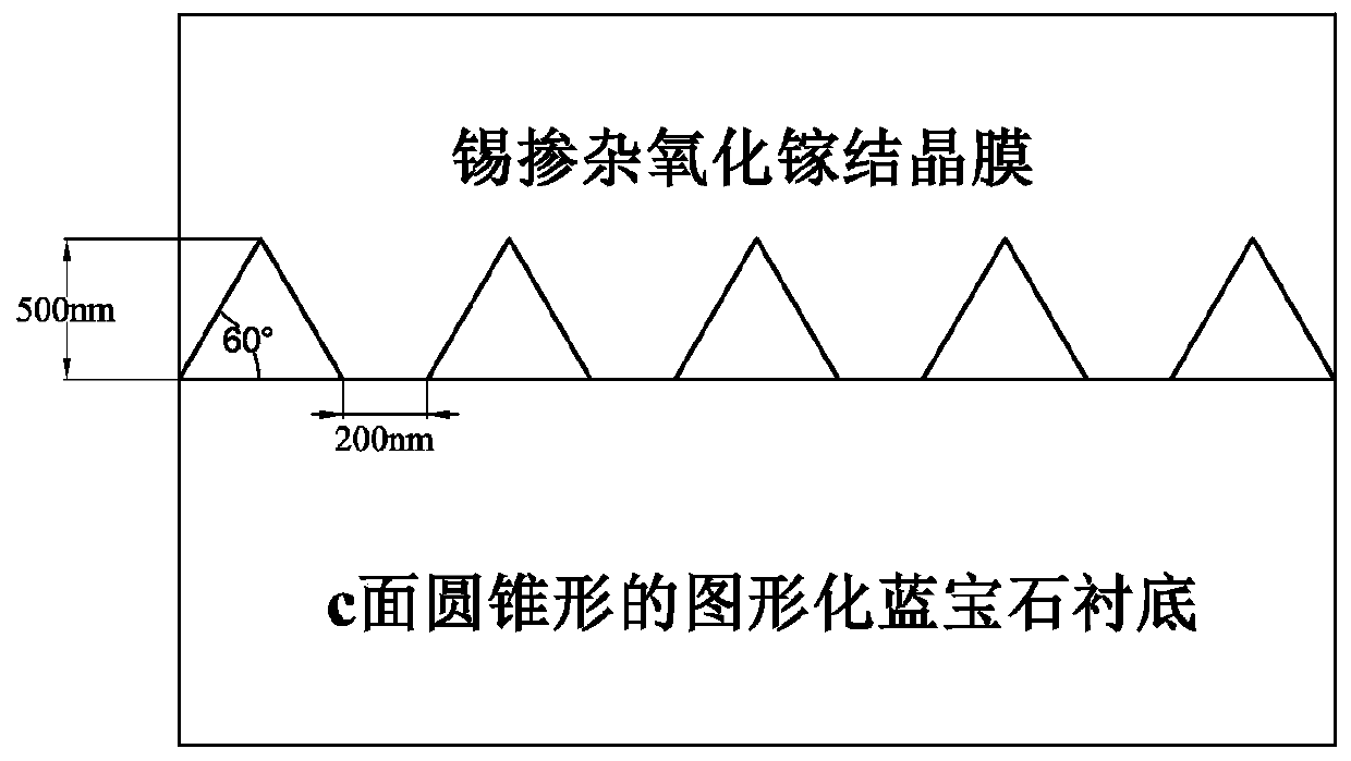
[0043] Using existing MOCVD equipment, organometallic trimethylgallium was used as the gallium source, oxygen was used as the oxygen source, tetrakis(dimethylamino)tin was used as the doping source, and argon with a purity of more than 99.999% was used as the carrier gas and growth protective atmosphere, High-quality tin-doped gallium oxide crystalline films were grown on conical patterned sapphire substrates.

[0044] The preparation method of the gallium oxide crystalline film is as follows:

[0045]Step 1: Select a patterned sapphire substrate with a c-plane conical shape, firstly, ultrasonically clean the substrate in acetone solution for 3-10min; secondly, ultrasonically clean it in isoacetone solution for 3-10min; The substrate is ultrasonically cleaned in hydrochloric acid and hydrogen peroxide solution, sulfuric acid and hydrogen peroxide solution for 3-10 minutes, and finally the substrate is taken out and then blown dry with nitrogen gas to complete the cleaning.

...

Embodiment 2

[0056] Using the existing MOCVD equipment, organometallic triethylgallium as the gallium source, deionized water as the oxygen source, argon with a purity of more than 99.999% as the carrier gas and growth protective atmosphere, the hexagonal patterned sapphire substrate was A gallium oxide crystalline film is grown thereon.

[0057] The preparation method of the gallium oxide crystalline film is as follows:

[0058] Step 1: Select a c-plane hexagonal patterned sapphire substrate, firstly, ultrasonically clean the substrate in acetone solution for 3-10min; secondly, ultrasonically clean it in isoacetone solution for 3-10min; The substrate is ultrasonically cleaned in hydrochloric acid, hydrogen peroxide solution, sulfuric acid and hydrogen peroxide solution for 3-10 minutes, and finally the substrate is taken out and then blown dry with nitrogen gas to complete the cleaning.

[0059] Step 2: Control the MOCVD equipment, send the substrate into the reaction chamber, and rotate...

Embodiment 3

[0071] Compared with Example 1, other conditions are the same, except that the substrate adopts a c-plane hemispherical patterned sapphire substrate.

[0072] see Figure 8 , is a schematic diagram of the stacked structure of growing gallium oxide crystalline film on a hemispherical patterned sapphire substrate.


PUM

PropertyMeasurementUnit
thicknessaaaaaaaaaa
thicknessaaaaaaaaaa
heightaaaaaaaaaa

Abstract

The invention provides a gallium oxide semiconductor laminated structure. The gallium oxide semiconductor laminated structure comprises a patterned sapphire substrate and a gallium oxide crystal filmgrown on the patterned sapphire substrate. The gallium oxide is pure-phase or pure-phase gallium oxide. An actual surface and a c crystal face of the patterned sapphire substrate have a deviation angle of 0-10 degrees, and the thickness of the patterned sapphire substrate is 400 micrometers to 2 millimeters. The graphical sapphire substrate is in one of a groove shape, a hexagon shape, a trilateral shape, a hemisphere shape, a cone shape, a pyramid shape, a circular truncated cone shape, a hexagonal pyramid shape, a triangular pyramid shape or a triangular truncated cone shape or more, and theheight of the graphical structure is 100 nanometers to 2 micrometers. According to the invention, the problem that a mixed phase is easily generated in the process of growing a phase or phase galliumoxide on a heterogeneous substrate is solved, and pure-phase gallium oxide or pure-phase gallium oxide can be obtained on the heterogeneous substrate.

Description

technical field [0001] The invention belongs to the technical field of semiconductor materials and semiconductor optoelectronic devices, and mainly relates to a laminated structure containing a gallium oxide crystalline film and a preparation method thereof. Background technique [0002] In recent years, wide-bandgap semiconductor materials represented by gallium nitride and silicon carbide have been widely used in the preparation of high-power and high-frequency devices. The band gap of gallium oxide is higher than that of gallium nitride and silicon carbide, and it has a higher breakdown voltage. And the Barriga figure of merit of gallium oxide, as a low loss index, is more than four times that of gallium nitride and silicon carbide, indicating that gallium oxide material will have better device performance in high-power electronic devices. [0003] According to the classification of crystal structure, gallium oxide has various isomers, which are respectively recorded as ...

Claims


Application Information

Patent Timeline
Patent Type & Authority Patents(China)
IPC IPC(8): H01L33/22H01L33/00
CPCH01L33/005H01L33/22
Inventor 王钢李泽琦陈梓敏
Owner 上海您惦半导体科技有限公司
Why Eureka
Try Eureka