
A method of controlling the texture of vapor-deposited metal thin films by using semiconductor substrates

A metal thin film, vapor deposition technology, applied in metal material coating process, vacuum evaporation coating, coating and other directions, can solve the problems of complex process, instability, high cost of single crystal preparation, etc. tiny effect

Active Publication Date: 2020-10-30
TIANJIN UNIV
View PDF3 Cites 0 Cited by
  • Summary
  • Abstract
  • Description
  • Claims
  • Application Information

AI Technical Summary

Problems solved by technology

It can be seen that the traditional method of changing the deposition parameters cannot well control the texture of the film during vapor deposition, the texture change is not obvious or unstable, and even if the texture of the grown film can be changed by changing the deposition airflow, substrate temperature and other conditions , often these deposition parameters are not well applicable to all vapor deposition equipment, and the way to control the texture is more complicated, which is easy to cause waste of resources and low yield
If the traditional method of epitaxial growth is used to change the film growth texture, a single crystal substrate is often required, and the cost of single crystal preparation is high and the process is complicated.
If the subsequent heat treatment is used to change the texture of the deposited film, there will be disadvantages such as increased procedures and increased energy consumption.

Method used


Image

  • A method of controlling the texture of vapor-deposited metal thin films by using semiconductor substrates
  • A method of controlling the texture of vapor-deposited metal thin films by using semiconductor substrates
  • A method of controlling the texture of vapor-deposited metal thin films by using semiconductor substrates

Examples


Embodiment 1

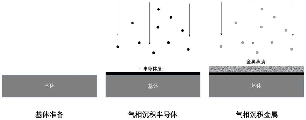
[0031] The metal Al thin film was vapor-deposited by Knudsen evaporation source by means of thermal evaporation. First prepare an inert SiO 2 The substrate of the oxide layer was cleaned with acetone and isopropanol in an ultrasonic cleaner, and then dried with pressurized nitrogen. The background vacuum of the vacuum chamber is 10 -8 Pa, the deposition temperature is room temperature. Next, a layer of Ge is thermally evaporated and deposited on the substrate in advance, with a deposition thickness of 1 nm. Finally, on the basis of the Ge substrate, continue to thermally evaporate the Al thin film, and the deposition thickness is 100nm.

[0032] Also using the thermal evaporation method, first prepare an inert SiO 2 The substrate of the oxide layer was cleaned with acetone and isopropanol in an ultrasonic cleaner, and then dried with pressurized nitrogen. The background vacuum of the vacuum chamber is 10 -8 Pa, the deposition temperature is room temperature. directly on...

Embodiment 2

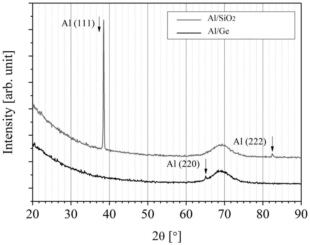
[0035] The metal Al thin film was vapor-deposited by Knudsen evaporation source by means of thermal evaporation. First prepare an inert SiO 2 The substrate of the oxide layer was cleaned with acetone and isopropanol in an ultrasonic cleaner, and then dried with pressurized nitrogen. The background vacuum of the vacuum chamber is 10 -7 Pa, the deposition temperature is room temperature. Next, a layer of Ge is preliminarily thermally evaporated on the substrate with a deposition thickness of 10 nm. Finally, on the basis of the Ge substrate, continue to thermally evaporate the Al thin film, and the deposition thickness is 1000nm. The prepared Al / Ge film exhibits (110) texture.

Embodiment 3

[0037] The metal Al thin film was vapor-deposited by Knudsen evaporation source by means of thermal evaporation. First prepare an inert SiO 2 The substrate of the oxide layer was cleaned with acetone and isopropanol in an ultrasonic cleaner, and then dried with pressurized nitrogen. The background vacuum of the vacuum chamber is 5×10 -8 Pa, the deposition temperature is room temperature. Next, a layer of Ge is thermally evaporated and deposited on the substrate in advance, with a deposition thickness of 50 nm. Finally, on the basis of the Ge substrate, continue to thermally evaporate the Al thin film, and the deposition thickness is 500nm. The prepared Al / Ge film exhibits (110) texture.


PUM

PropertyMeasurementUnit
particle sizeaaaaaaaaaa

Abstract

The invention relates to a vapor deposition metal film texture regulated and controlled by a semiconductor substrate and a preparation method. The preparation method comprises the steps that a non-semiconductor substrate is prepared, and a target metal film is formed on the surface of the semiconductor substrate through deposition. A semiconductor is Ge or Si or Si-Ge alloy. The deposit target metal can be pure metal or alloy, and at least includes one of the following metal elements including Al, Au, Ni, Cu, Pt, Pd and Bi. According to the preparation method, the deposition mode is simple, and the texture change is obvious. A semiconductor layer can be easily formed through deposition before deposition of the metal film is conducted, and therefore the growth mode of the film texture can be obviously changed, the regulation and control success rate of the film texture is high, complicated adjustment of deposition parameters is not required, and an expensive single crystal substrate required by an epitaxial growth method is not required. An Al deposition film in the specific scheme only needs to form on a Ge substrate through deposition so that the texture of the Al deposition filmcan be turned into a special high energy face (110) from a conventional low energy face (111).

Description

technical field [0001] The invention belongs to the field of metal thin film material preparation, and in particular relates to a method for regulating the texture and preparation of a metal thin film by using a semiconductor substrate. [0002] technical background [0003] As an important component in the field of modern industrial technology, vapor-deposited metal thin film materials are widely used in catalytic reactions, integrated circuits, information storage, displays, sensors, etc. Thin films grown by various atomic deposition techniques are generally polycrystalline with specific textures. Texture changes are crucial to the development of the properties of metallic thin films. For example, the elastic modulus of the metal copper film on the <111> crystal direction is 2.9 times that of the <110> crystal direction [Deformation and fracture mechanics of engineering materials, Wiley, New York, 1996]; on the copper (110) plane its oxide , The catalytic reac...

Claims


Application Information

Patent Timeline
Patent Type & Authority Patents(China)
IPC IPC(8): C23C14/16C23C14/18C23C14/24C23C14/35
CPCC23C14/16C23C14/18C23C14/24C23C14/35
Inventor 王祖敏王璟刘永长赵欢欢刘晨曦余黎明
Owner TIANJIN UNIV
Learn More