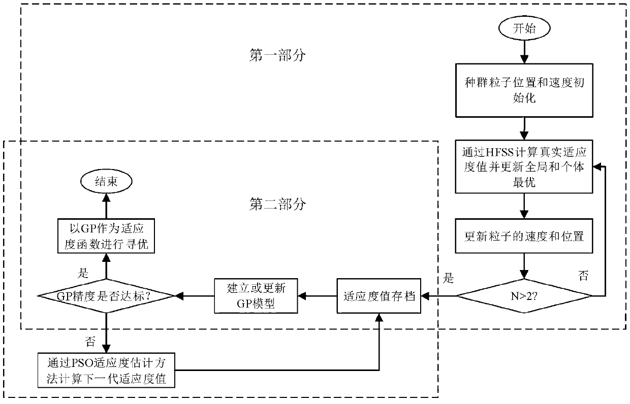
Antenna rapid optimization design method
An optimized design and antenna technology, applied in the field of Gaussian process modeling for antenna design, rapid antenna design, can solve problems such as high calculation cost and large data volume
- Summary
- Abstract
- Description
- Claims
- Application Information
AI Technical Summary
Problems solved by technology
Method used
Image
Examples
Embodiment 1
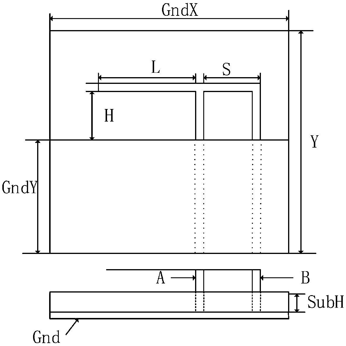
[0102] Design an inverted F antenna as figure 2 As shown, where A is the excitation port, B is the ground hole, the optimization design index is the return loss at the resonance frequency S 11 Less than -20dB, and its -10dB bandwidth is greater than 100MHz. When designing an inverted-F antenna, the resonant length L of the antenna, the height H of the antenna and the distance S between the two vertical arms determine the input impedance, resonant frequency, and antenna bandwidth of the antenna. The constant size parameters are shown in Table 1.
[0103] Table 1 Inverted-F Antenna Structure Parameters
[0104]
[0105] Specific steps are as follows:
[0106] (1) Establish the model of HFSS, such as image 3 As shown, the material of the dielectric layer is the most commonly used glass fiber epoxy resin (FR4) in PCB, and its relative dielectric constant ε r =4.4, tanδ=0.02.
[0107] (2) Population particle position and velocity initialization: adopt the method of ortho...
Embodiment 2
[0113] Design a GPS Beidou dual-mode microstrip antenna, such as Figure 6 As shown, the optimal design index is: at 1.561GHz (Beidou B1 operating frequency) and 1.573GHz (GPSL1 operating frequency), the VSWR is less than or equal to 1.5, at 1.561GHz (Beidou B1 operating frequency) and 1.573GHz (GPSL1 operating The polarization at frequency) is right-handed circular polarization and the polarization gain is greater than or equal to 4dBic. In this example, by optimizing W, L 1 , L 2 To achieve the design index, the values of each parameter are shown in Table 2.
[0114] Specific steps are as follows:
[0115] (1) Establish the model of HFSS, such as Figure 7 As shown, the dielectric substrate material is the relative permittivity of ε r =4.5 Arlon AD450, the top of the dielectric plate is covered with a square radiation patch, and the four sides of the patch are two kinds of branches with the same width and different lengths. These two branches correspond to the two wo...
PUM
 Abstract
Description
Claims
Application Information
 - R&D
- Intellectual Property
- Life Sciences
- Materials
- Tech Scout
- Unparalleled Data Quality
- Higher Quality Content
- 60% Fewer Hallucinations
Browse by: Latest US Patents, China's latest patents, Technical Efficacy Thesaurus, Application Domain, Technology Topic, Popular Technical Reports.
© 2025 PatSnap. All rights reserved.Legal|Privacy policy|Modern Slavery Act Transparency Statement|Sitemap|About US| Contact US: help@patsnap.com


