A Method for Extracting Radiation Defects from Linear Circuits
A linear circuit and extraction method technology, applied in the direction of electronic circuit testing, measuring electricity, measuring electrical variables, etc., can solve problems such as inability to separate discrete devices, achieve enrichment of low dose rate enhancement effects, reduce quantity, improve speed and accuracy Effect
- Summary
- Abstract
- Description
- Claims
- Application Information
AI Technical Summary
Problems solved by technology
Method used
Image
Examples
Embodiment 1
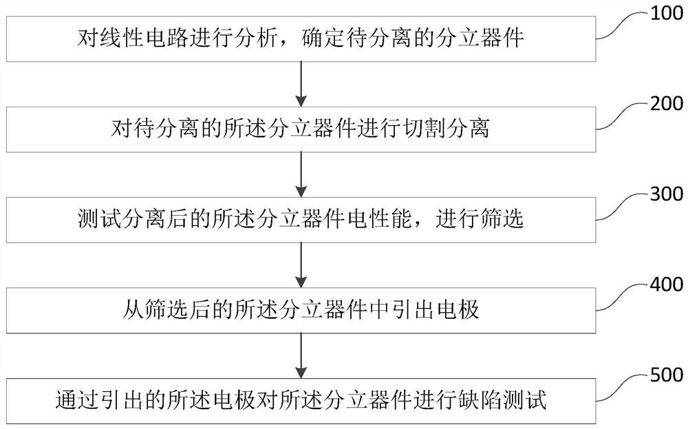
[0045] Such as figure 1 As shown, it is; Wherein, the linear circuit radiation defect extraction method includes:
[0046] Step 100, analyzing the linear circuit to determine the discrete device to be separated;
[0047] Analyze the linear circuit. Under the influence of external radiation, the overall performance of the linear circuit itself degrades, and the circuit parameters change greatly. Through the analysis of the linear circuit, the purpose is to preliminarily determine that the large change in parameters may be due to the linear circuit. Which discrete devices are caused by these discrete devices, and these discrete devices that may affect large changes in parameters are discrete devices that need to be independently extracted for defects, that is, discrete devices to be separated.
[0048] Step 200, cutting and separating the discrete device to be separated;
[0049] By cutting, the discrete devices to be separated are separated, so that the separated discrete dev...
Embodiment 2
[0092] The difference between this embodiment and the above-mentioned linear circuit radiation defect extraction method is that the linear circuit 7J139 is taken as an example in this embodiment to describe the linear circuit radiation defect extraction method.
[0093] The defect extraction process using linear circuits is as follows:
[0094] (1) Clarify the size of the circuit die (discrete device size), the die size of 7J139 is: 1.03mm×1.00mm×0.32mm, the layout of the die is as follows Figure 6 shown.
[0095] (2) Label the internal units of the die and determine the schematic diagram. The die layout after the label is as follows Figure 7 As shown (wherein, the labels in the figure are for distinguishing during the radiation defect extraction process, and are not the reference signs of this application), for the 7J139 circuit, there are 14 lead-out terminals, 8 vertical PNP tubes, and horizontal PNP tubes. There are 17 tubes, 8 diodes formed by horizontal PNP tubes, 1...
PUM
 Abstract
Description
Claims
Application Information
 - R&D Engineer
- R&D Manager
- IP Professional
- Industry Leading Data Capabilities
- Powerful AI technology
- Patent DNA Extraction
Browse by: Latest US Patents, China's latest patents, Technical Efficacy Thesaurus, Application Domain, Technology Topic, Popular Technical Reports.
© 2024 PatSnap. All rights reserved.Legal|Privacy policy|Modern Slavery Act Transparency Statement|Sitemap|About US| Contact US: help@patsnap.com


