Integrated sorting device for single cell Raman measurement and laser microscopic cutting
A laser microdissection and sorting device technology, which is applied in measuring devices, Raman scattering, individual particle analysis, etc., can solve problems affecting molecular operations, cell activity damage, etc.
- Summary
- Abstract
- Description
- Claims
- Application Information
AI Technical Summary
Problems solved by technology
Method used
Image
Examples
Embodiment 1
[0039] Embodiment 1: Material selection and fabrication of Raman measurement and laser microdissection thin film
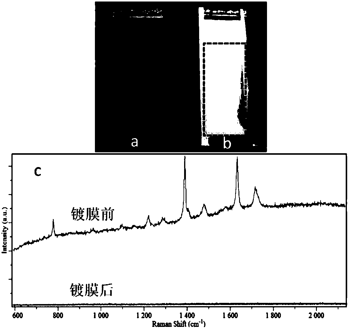
[0040] Raman measurement and laser microdissection of thin films including cut layer and Raman coating. Among them, the cutting layer ( figure 1 a) Using laser-sensitive polymer materials, including but not limited to PC (polycarbonate), EVA (ethylene-vinyl acetate copolymer), PET (polyethylene terephthalate), PEN (polyethylene naphthalate) glycol esters); Raman coatings are made of opaque metallic materials, including but not limited to aluminum, silver, gold. The Raman coating is formed on the surface of the cutting layer by deposition methods such as evaporation and sputtering ( figure 1 b), the thickness of the Raman coating is made to be 10-100nm. The Raman coating itself has no Raman background, and can cover the Raman background of the cutting layer (such as figure 1 shown in c).
Embodiment 2
[0041] Example 2: Fabrication of cell spotting chip, cell recovery chip and integrated device assembly
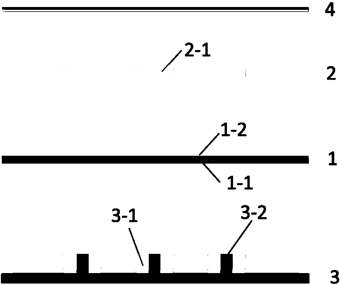
[0042] The cell spotting chip 2 is made of transparent soft polymer materials, including but not limited to PDMS (polydimethylsiloxane), silicone rubber, PVC (polyvinyl chloride), and the thickness is 0.2-2mm. For the through hole 2-1, the diameter of the micro through hole is made to be 0.5-5mm.
[0043] The cell recovery chip 3 is made of transparent materials, including but not limited to silicate glass, PDMS (polydimethylsiloxane), PMMA (polymethyl methacrylate); the chip contains a microwell 3-1 structure with a certain depth In the center of the micro-well 3-1, a micro-column 3-2 with the same height as the micro-well 3-1 is made, and the surface of the micro-column has a certain degree of adhesion. The positions of the microwells 3-1 and the microcolumns 3-1 on the cell recovery chip 3 are in one-to-one correspondence with the positions of the microthrough holes 2-1...
Embodiment 3
[0045] Example 3: Using an integrated device for single-cell Raman measurement and cell sorting
[0046] In the above-mentioned integrated device, a 532nm high-energy pulsed laser can be used for laser microdissection of the Raman measurement and laser microdissection film, and then the cells are separated separately to recover the chip. Due to the adhesion of the microcolumn, the cut Raman measurement And the laser microdissection film 1 remains on the surface of the microcolumn during separation, thereby realizing the separation and recovery of the cut area, wherein, image 3 a is the Raman measurement and laser microdissection film 1 area map after laser cutting, image 3 b is the separated Raman measurement and laser microdissection film 1 area map, image 3 c is the cut Raman measurement and laser microdissection film 1 area diagram of the adhered micropillar 3-2, and the circle area shows the surface of the micropillar. When separating cells, the cell suspension is dri...
PUM
| Property | Measurement | Unit |
|---|---|---|
| Thickness | aaaaa | aaaaa |
| Thickness | aaaaa | aaaaa |
| Wavelength | aaaaa | aaaaa |
Abstract
Description
Claims
Application Information
 - R&D
- Intellectual Property
- Life Sciences
- Materials
- Tech Scout
- Unparalleled Data Quality
- Higher Quality Content
- 60% Fewer Hallucinations
Browse by: Latest US Patents, China's latest patents, Technical Efficacy Thesaurus, Application Domain, Technology Topic, Popular Technical Reports.
© 2025 PatSnap. All rights reserved.Legal|Privacy policy|Modern Slavery Act Transparency Statement|Sitemap|About US| Contact US: help@patsnap.com


