A method of electrodepositing wo3 thin film on discontinuous conductive film
A conductive film and electrodeposition technology, applied in non-woven fabrics, superimposed layer coating, electrolytic inorganic material coating and other directions, can solve the problem of high cost of preparation methods, and achieve the effects of low cost, large optical modulation, and large control window.
- Summary
- Abstract
- Description
- Claims
- Application Information
AI Technical Summary
Problems solved by technology
Method used
Image
Examples
Embodiment 1
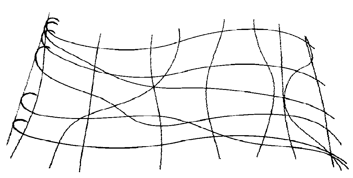
[0042] (1) figure 1 It is a schematic structural diagram of the W / Ag NTs / W / PET transparent conductive film of the present invention. A commercially available PET (or other flexible substrate) flexible film (light transmittance ~ 95%) with a thickness of 100 μm was cut into small rectangular pieces, and the surface of the PET was ultrasonically cleaned with ethanol and water respectively, and used as a substrate for future use. Then fix it in the chamber of the magnetron sputtering instrument, pass in argon gas, set the sputtering parameters as pressure 4-6Pa, power 60-100W, sputtering time 1-10min for WO 3 Sputtering of the base layer.
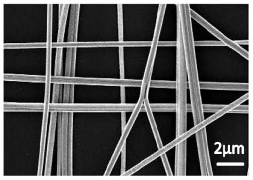
[0043] (2) PVA nanofibers were prepared by electrospinning, and the grooves made of thick aluminum foil were used as PVA spinning receivers. The PVA solution is used as the spinning ink, and the spinning is carried out perpendicular to the groove in an electric field with a positive voltage of 10-15kV and a negative voltage of 0-2kV. The ob...
Embodiment 2
[0048] Step (1), (2) are identical with embodiment 1.
[0049] (3) H with a ratio of 1:4:50 2 o 2 : HClO 4 : DI water is added into the beaker and mixed to obtain the deposition solution. Put the conductive substrate obtained in step (3) into the deposition solution, and set the parameters on the electrochemical workstation to deposit WO 3 , the pulse voltage of each cycle is: -1V, 0.1s, 0V, 0.5s and the cycle interval of 1.1 ~ 1.5s. Set the total deposition time to 1.5 h. from Figure 7 It can be seen that as the deposition time increases, the discoloration window of the film increases to 80.6%.
[0050] (4) This step is the same as step (4) in Example 1.
[0051] The discoloration window test curve of the sample prepared in the embodiment of the present invention 2 sees Image 6 .
Embodiment 3
[0053] Steps (1) and (2) are the same as in Example 1.
[0054] (3) H with a ratio of 1:4:50 2 o 2 : HClO 4 : DI water is added into the beaker and mixed to obtain the deposition solution. Put the conductive substrate obtained in step (3) into the deposition solution, and set the parameters on the electrochemical workstation to deposit WO 3 , the pulse voltage of each cycle is: -1V, 0.1s, 0V, 0.5s and the cycle interval of 1.1 ~ 1.5s. Set the total deposition time to 2h. from Figure 8 It can be seen that as the deposition time increases, the film thickness increases, and the discoloration window of the film increases to 89.7%.
[0055] (4) This step is the same as step (4) in Example 1.
[0056] The discoloration window test curve of the sample prepared in the embodiment of the present invention 3 sees Figure 7 , the SEM of the different magnifications of the sample prepared in the embodiment of the present invention 3 sees Figure 8 .
PUM
| Property | Measurement | Unit |
|---|---|---|
| thickness | aaaaa | aaaaa |
| height | aaaaa | aaaaa |
| thickness | aaaaa | aaaaa |
Abstract
Description
Claims
Application Information
 - R&D
- Intellectual Property
- Life Sciences
- Materials
- Tech Scout
- Unparalleled Data Quality
- Higher Quality Content
- 60% Fewer Hallucinations
Browse by: Latest US Patents, China's latest patents, Technical Efficacy Thesaurus, Application Domain, Technology Topic, Popular Technical Reports.
© 2025 PatSnap. All rights reserved.Legal|Privacy policy|Modern Slavery Act Transparency Statement|Sitemap|About US| Contact US: help@patsnap.com


