A method for preparing large-area high-quality graphene
A graphene, high-quality technology, applied in the field of functional thin film material preparation, can solve the problems of low growth rate of graphene, increase of uncontrollable growth process, difficulty in large-scale preparation of high-quality graphene, etc., to achieve nucleation and growth process Controllable, realize the effect of industrialized preparation and rapid preparation
- Summary
- Abstract
- Description
- Claims
- Application Information
AI Technical Summary
Problems solved by technology
Method used
Image
Examples
Embodiment 1
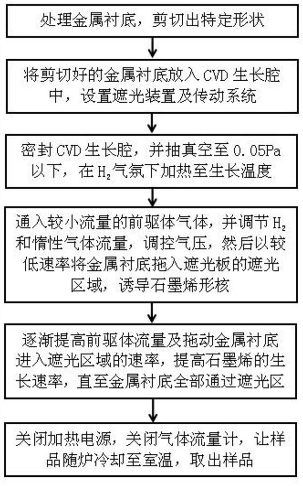
[0029] A method for preparing large-area high-quality graphene (preparing large-area high-quality graphene on a 25 μm thick copper foil substrate), comprising the following steps:
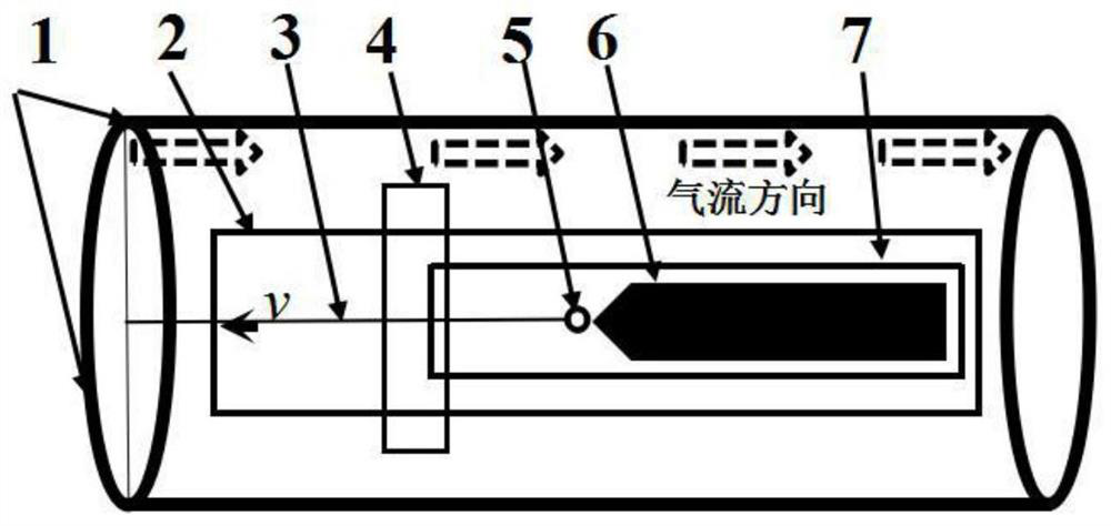
[0030] 1) Place the metal copper foil substrate. First, place the quartz plate 2 in the heating zone of the quartz tube 1 of the chemical vapor deposition system; 2, and connected to the transmission nickel wire 3 of the transmission system through the round hole 5; again, the 25 μm thick copper foil substrate 6 is placed flat on the nickel foil 7, and the tip of the copper foil substrate 6 is in the same direction as the air inlet ; Then place the light-shielding plate nickel foil 4 on the left end 1 / 5 of the quartz plate 2 to form a shielding area; finally, seal the growth chamber;
[0031] 2) Turn on the vacuum pump and pump the pressure in the growth chamber to below 0.01Pa;
[0032] 3) Infuse 2.5 sccm of high-purity hydrogen with a pressure of 0.5 Pa, turn on the heating power, and heat the g...
Embodiment 2
[0043] A method for preparing large-area high-quality graphene (preparation of large-area high-quality graphene on a 25 μm thick surface copper oxide foil substrate)
[0044] 1) Place the surface oxide copper foil substrate, at first, place the quartz plate 2 on the heating zone of the quartz tube 1 of the CVD system; then, place the nickel foil 7 with a round hole at one end on the quartz plate 2, and pass The round hole 5 is connected to the transmission nickel wire 3 of the transmission system; again, the surface oxide copper foil substrate 6 with a thickness of 25 μm is placed flat on the nickel foil 7, and the tip of the surface oxide copper foil substrate 6 is in the same direction as the air inlet; Then place the light-shielding nickel foil 4 on the left end 1 / 5 of the quartz plate 2; finally, seal the growth chamber;
[0045] 2) Turn on the vacuum pump and pump the pressure in the CVD growth chamber to 0.04Pa;
[0046] 3) Pass into the high-purity H of 250sccm 2 , th...
Embodiment 3
[0054] A method for preparing large-area high-quality graphene (preparation of large-area high-quality graphene on a 25 μm thick surface copper oxide foil substrate)
[0055] 1) Place the surface oxide copper foil substrate. First, place the quartz plate 2 in the heating zone of the quartz tube 1 of the CVD system; , and connected to the transmission nickel wire 3 of the transmission system through the round hole 5; again, the 25 μm thick surface oxide copper foil substrate 6 is placed flat on the nickel foil 7, wherein the tip of the surface oxide copper foil substrate 6 is connected to the air inlet The direction is the same; then the light-shielding nickel foil 4 is placed on the left end 1 / 5 of the quartz plate 2; finally, the growth chamber is sealed;
[0056] 2) Turn on the vacuum pump and pump the pressure in the CVD growth chamber to 0.04Pa;
[0057] 3) Introduce high-purity hydrogen with a flow rate of 500 sccm and a pressure of 10 5 Pa, and turn on the heating powe...
PUM
| Property | Measurement | Unit |
|---|---|---|
| thickness | aaaaa | aaaaa |
Abstract
Description
Claims
Application Information
 - R&D
- Intellectual Property
- Life Sciences
- Materials
- Tech Scout
- Unparalleled Data Quality
- Higher Quality Content
- 60% Fewer Hallucinations
Browse by: Latest US Patents, China's latest patents, Technical Efficacy Thesaurus, Application Domain, Technology Topic, Popular Technical Reports.
© 2025 PatSnap. All rights reserved.Legal|Privacy policy|Modern Slavery Act Transparency Statement|Sitemap|About US| Contact US: help@patsnap.com


