Integrated circuit chip packaging structure and manufacturing method thereof

A technology of integrated circuit and packaging structure, which is applied in the direction of circuits, electrical components, electric solid devices, etc., can solve problems such as permanent failure, user loss, and short-term failure, so as to prolong low-temperature life, prevent short-term failure or permanent failure, and reduce low-temperature failure. The effect of error rate

Active Publication Date: 2019-02-19
SHANGHAI HUAHONG GRACE SEMICON MFG CORP
View PDF9 Cites 0 Cited by
  • Summary
  • Abstract
  • Description
  • Claims
  • Application Information

AI Technical Summary

Problems solved by technology

In extreme cases, there may even be a temporary failure or a permanent failure due to an irreversible internal mistriggered operation, resulting in user losses

Method used


Image

  • Integrated circuit chip packaging structure and manufacturing method thereof

Examples


Embodiment Construction

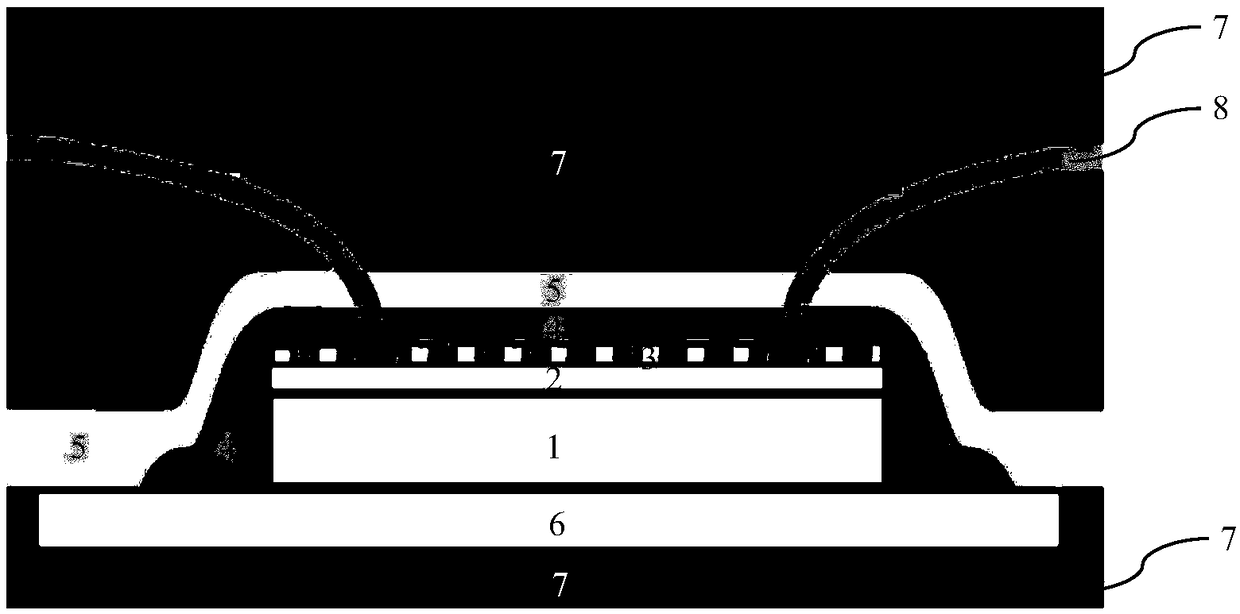
[0033] Such as figure 1 As shown, it is a schematic structural diagram of the packaging structure of the integrated circuit 2 chip 1 in the embodiment of the present invention. In the packaging structure of the integrated circuit 2 chip 1 in the embodiment of the present invention, the integrated circuit 2 on the chip 1 includes a temperature-sensitive circuit. Sensitive circuitry increases chance of failure as operating temperature decreases; package construction includes:

[0034] A heat conduction layer 4, the heat conduction layer 4 completely covers at least the front and side surfaces of the temperature sensitive circuit.

[0035] The heat insulating layer 5 is formed on the surface of the heat conducting layer 4 and covers the heat conducting layer 4 .

[0036] The heat-conducting layer 4 forms a structure that makes the temperature of each position of the area covered by the heat-conducting layer 4 uniform, and the heat-insulating layer 5 forms a structure that preven...


PUM


Abstract

The invention discloses an integrated circuit chip packaging structure. An integrated circuit on a chip comprises a temperature sensitive circuit, the failure probability of the temperature sensitivecircuit is increased when working temperature is reduced, the packaging structure comprises a heat conduction layer and a heat insulating layer, the heat conduction layer completely wraps the front and the side surface of the temperature sensitive circuit, the heat insulating layer is formed on the surface of the heat conduction layer and wraps the heat conduction layer, the heat conduction layerforms a structure, the temperatures of various positions of areas wrapped by the heat conduction layer are uniformed by the structure, the heat insulating layer forms a structure, the structure for preventing areas wrapped by the heat insulating layer from cooling, so that the temperatures of the areas wrapped by the heat insulating layer are kept by the structure, and lower temperature end of a working temperature range of the chip can be widened. The invention further discloses a manufacturing method of the integrated circuit chip packaging structure. According to the structure, heat loss ofthe chip can be reduced, and customer loss caused by abnormity of an integrated circuit at excessively low temperature is avoided.

Description

technical field [0001] The invention relates to the field of semiconductor integrated circuits, in particular to a packaging structure for integrated circuit chips. The invention also relates to a method for maintaining the temperature of the integrated circuit chip. Background technique [0002] Due to the changeable application environment of integrated circuit chips, when a low temperature environment occurs, the integrated circuit characteristics of the chip will shift. In extreme cases, there may even be a temporary failure or an irreversible operation triggered by an internal error, resulting in permanent failure, resulting in user losses. [0003] There are several known methods to maintain the temperature of the integrated circuit of the chip, such as the method of installing a heater outside the chip, the method of covering the entire circuit board with an insulating layer or the method of heating the liquid circulation system, etc., to help the chip maintain the w...

Claims


Application Information

Patent Timeline
Patent Type & Authority Applications(China)
IPC IPC(8): H01L23/34H01L23/373
CPCH01L23/345H01L23/3735H01L23/3737H01L2224/8592H01L2224/45144H01L2224/73265H01L2924/00014
Inventor 张雨田
Owner SHANGHAI HUAHONG GRACE SEMICON MFG CORP
Why Eureka
Try Eureka