Etching liquid for semiconductor substrate

An etchant and semiconductor technology, applied in the field of etchant for semiconductor substrates for solar cells, etch force recovery agent, and semiconductor substrates for solar cells, to achieve the effects of reducing waste water treatment load, low light reflectivity, and reducing production costs

Inactive Publication Date: 2019-02-05
SETTSU OIL MILL
View PDF14 Cites 0 Cited by
  • Summary
  • Abstract
  • Description
  • Claims
  • Application Information

AI Technical Summary

Problems solved by technology

However, there has not been a mass-producible texture technology that can stably express a reflectance of 10% or less (wavelength 600nm) and achieve high power generation efficiency.

Method used


Image

  • Etching liquid for semiconductor substrate
  • Etching liquid for semiconductor substrate
  • Etching liquid for semiconductor substrate

Examples


Embodiment 1~23 and comparative example 1~10

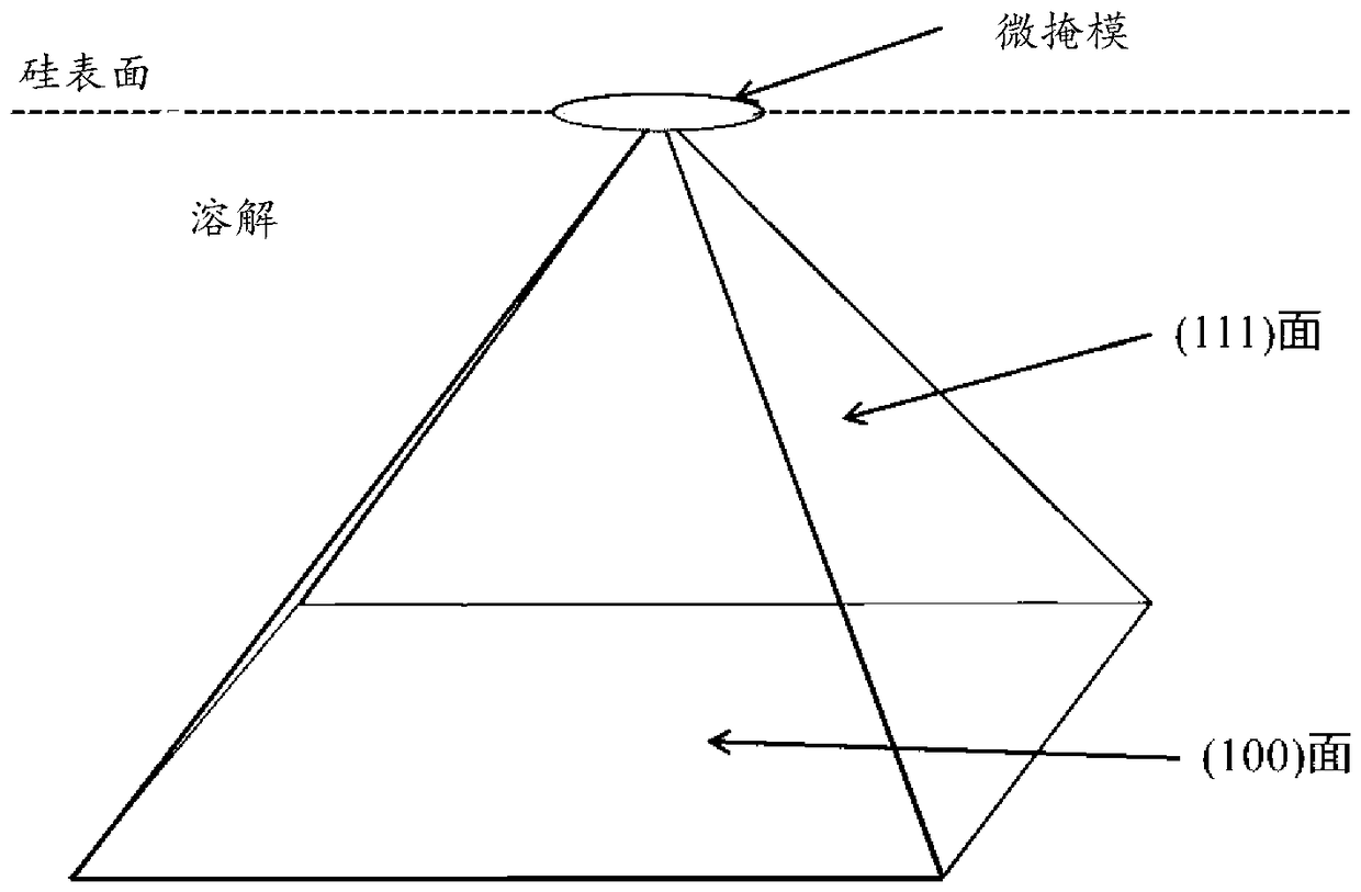
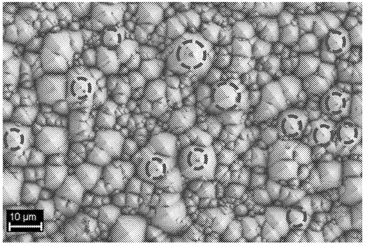
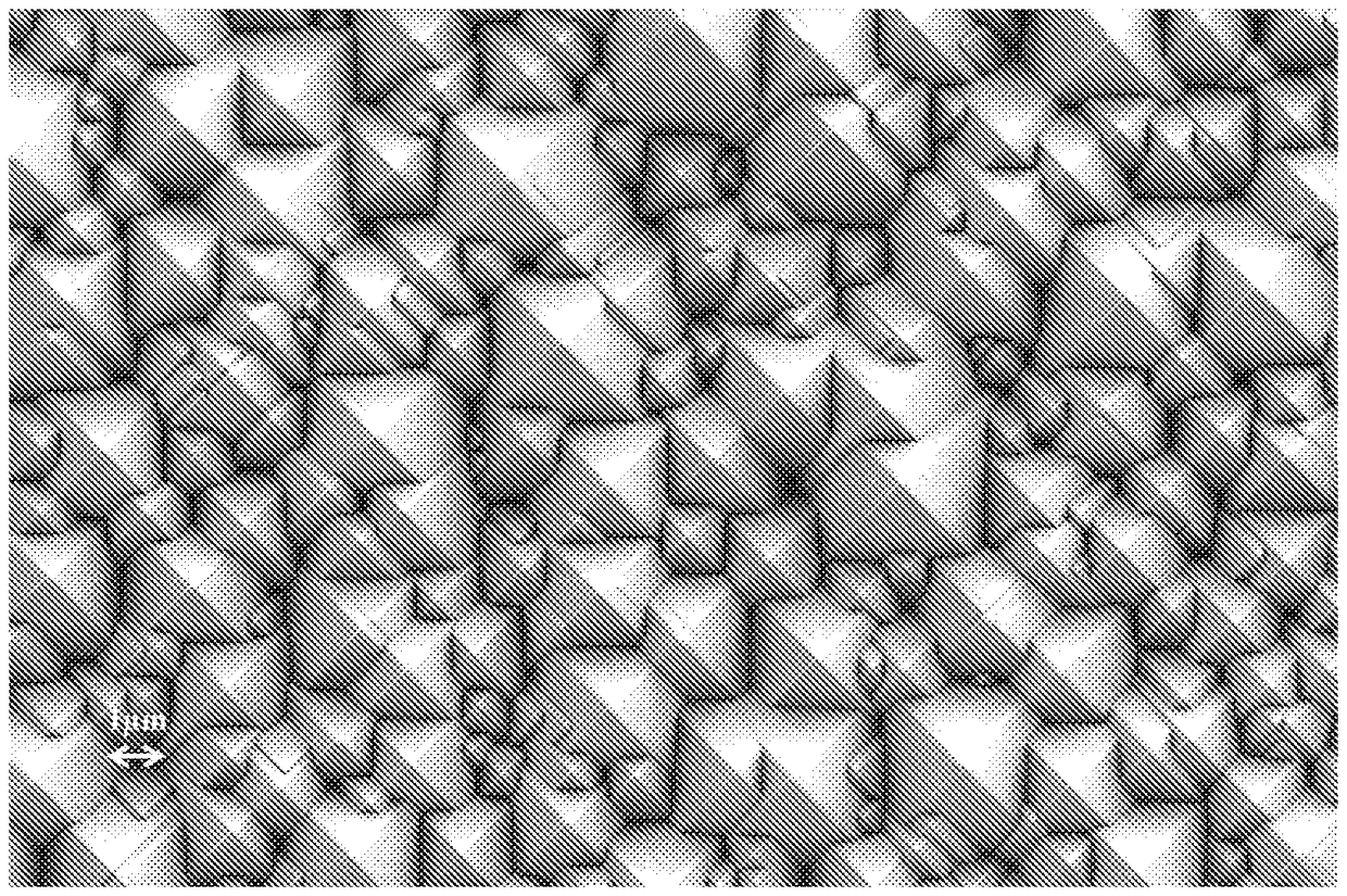
[0152] An n-type monocrystalline silicon substrate (a square with a side length of 125 mm and a thickness of 160 mm) with a crystal orientation (100) plane on the surface mu m substrate) in the conditions shown in Table 1A, that is, at 50 to 90° C., immersed in an etching solution prepared according to the blend composition shown in Table 1A for 1 to 40 minutes. The etched substrate surface was observed visually, with a laser microscope and a scanning electron microscope, and the results are shown in Table 1B. The chelating agent used (Additive 2) was DTPA (diethylenetriaminepentaacetic acid). In addition, the operation of a specific etching process is as described in the following [etching process]. The pH value of the etching solution in these examples and comparative examples is in the range of 12 to 14 at 25°C.

[0153] In addition, sodium sulfite (Example 2, Example 20, and Comparative Example 5) or sodium ascorbate (Example 10) was contained in the etching solution at ...


PUM

PropertyMeasurementUnit
sizeaaaaaaaaaa
thicknessaaaaaaaaaa
reflectanceaaaaaaaaaa

Abstract

The present invention provides an etching liquid, which is an alkaline etching liquid for treating the surface of a semiconductor substrate for solar cells, the alkaline etching liquid contains at least one hydroxystyrene-based polymer represented by general formula (1), the total amount of oligomers and monomers in which n is 1-8 contained in the hydroxystyrene-based polymer is no greater than 3.5% of the hydroxystyrene-based polymer. The present invention exhibits the effect of enabling texture formation on a semiconductor substrate for a solar cell in a shorter time at a relatively low temperature, exhibiting exceptional continuous producibility and product storage stability, and making it possible to stably obtain a surface having and low light reflectance. It is also possible to stably form pyramid-shaped recesses and projections of 3 [mu]m or less on average, and to stably impart surface shapes exhibiting a light reflectivity of 10% or less, which were unobtainable using the prior art, to a semiconductor substrate for a solar cell, without being affected by lot-to-lot fluctuations in the raw materials for the etching liquid.

Description

technical field [0001] The present invention relates to an etchant for a semiconductor substrate, particularly an etchant for a semiconductor substrate for a solar cell. The present invention also relates to an etching force recovery agent, a method for producing a semiconductor substrate for a solar cell, and a semiconductor substrate for a solar cell. Background technique [0002] In order to improve the power generation efficiency of a solar cell, a method of forming irregularities on the surface of a semiconductor substrate for a solar cell to efficiently collect (absorb) incident light from the substrate surface into the interior of the substrate is currently used. As a method for uniformly forming fine unevenness on the substrate surface, for example, a method is known in which the (100) plane of a single crystal silicon substrate is subjected to anisotropic etching using a mixed aqueous solution of sodium hydroxide and isopropanol to form a surface formed by ( 111) P...

Claims


Application Information

Patent Timeline
Patent Type & Authority Applications(China)
IPC IPC(8): H01L21/308H01L31/0236
CPCH01L21/308H01L31/0236Y02E10/50Y02P70/50
Inventor 赤木成明镰田义辉大八木伸斋田利典山本裕三
Owner SETTSU OIL MILL
Why Eureka
Try Eureka