A single photon avalanche diode with high detection efficiency and its manufacturing method

A single-photon avalanche and detection efficiency technology, applied in the field of single-photon detection, can solve the problems of low detection sensitivity and photon detection efficiency, and achieve the effects of increasing light transmittance, increasing width, and uniform electric field

Active Publication Date: 2020-01-21
南通三彩集成光电科技有限公司
View PDF4 Cites 0 Cited by
  • Summary
  • Abstract
  • Description
  • Claims
  • Application Information

AI Technical Summary

Problems solved by technology

[0003] The traditional single photon avalanche photodiode structure is composed of a planar single junction, which is generally a shallow junction structure. Generally low efficiency

Method used


Image

  • A single photon avalanche diode with high detection efficiency and its manufacturing method

Examples


Embodiment Construction

[0032] The present invention will be further described below in conjunction with accompanying drawing.

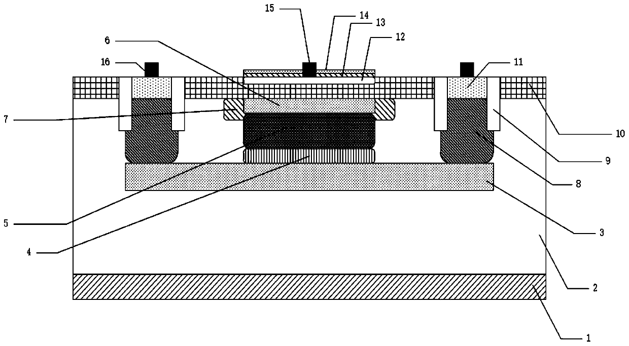
[0033] Such as figure 1 As shown, the single photon avalanche diode with high detection efficiency includes coaxially arranged p-substrate layer 1, p epitaxial layer 2, n+ buried layer 3, n-type charge layer 4, inversion deep n well 5, p-type charge layer 6. P-type semiconductor layer 7, n well layer 8, shallow trench isolation layer 9, p-type semiconductor layer 10, n+ type semiconductor layer 11, p+ type light absorbing layer 12, silicon dioxide anti-reflection film 13, nitrided Silicon antireflection film 14 , anode electrode 15 and cathode electrode 16 .

[0034] The p-substrate layer 1 is arranged at the bottom of the p-epitaxial layer 2 . A disk-shaped n+ buried layer 3 is provided inside the p epitaxial layer 2 . An n-type charge layer 4 , an inversion deep n well 5 , a p-type charge layer 6 , a p-type semiconductor layer 7 and an n-well layer 8 are arranged betwe...


PUM

PropertyMeasurementUnit
external quantum efficiencyaaaaaaaaaa

Abstract

The invention discloses a single photon avalanche diode with high detection efficiency and a manufacturing method thereof. The multiplication region of the traditional single photon avalanche photodiode is relatively thin, which leads to commonly low detection sensitivity and photon detection efficiency. The single photon avalanche diode with high detection efficiency comprises a p- substrate layer, a p epitaxy layer, an n+ buried layer, an n-type charge layer, an inverted deep n well, a p-type charge layer, a p- semiconductor layer, an n well layer, shallow groove isolation layers, a p-type semiconductor layer, an n+ semiconductor layer, a p+ light absorption layer, a silicon dioxide anti-reflection film, a silicon nitride anti-reflection film, an anode electrode and cathode electrodes which are arranged coaxially. The p+ light absorption layer, the p-type semiconductor layer and the p-type charge layer are adopted to form a p+ / p / p-type charge layer structure, current can expand horizontally first and then flow to the avalanche multiplication region, the spectral response is increased, and the absorption of the light wavelength by the single photon avalanche diode can be effectively improved.

Description

technical field [0001] The invention belongs to the technical field of single photon detection, and in particular relates to a single photon avalanche diode with high detection efficiency and a manufacturing method thereof. Background technique [0002] Single-photon detection technology is a very low-light detection and sensing technology, which has been widely used in contemporary life, such as in bioluminescence, quantum communication, astronomical research, and high-sensitivity sensors. As the core device of single photon detection, the single photon avalanche diode based on CMOS technology has attracted more and more attention and attention of researchers. Among them, the photon detection efficiency (Photon Detection Efficiency, PDE) is a key factor to measure the single photon detection ability of the avalanche photodiode. Therefore, designing a device structure with high photon detection efficiency is of great significance and use value. [0003] The traditional sin...

Claims


Application Information

Patent Timeline
Patent Type & Authority Patents(China)
IPC IPC(8): H01L29/861H01L21/329H01L29/06H01L27/144
CPCH01L27/1443H01L29/0684H01L29/66113H01L29/861
Inventor 张钰许明珠赵巨峰崔光茫逯鑫淼
Owner 南通三彩集成光电科技有限公司
Why Eureka
Try Eureka