Power circuit and semiconductor integration circuit device

A technology of integrated circuits and power circuits, which is applied in semiconductor/solid-state device manufacturing, circuits, electrical components, etc., can solve problems such as difficulty in repairing, waste of resources, etc., and achieve the effect of speeding up air-drying, saving time and cost, and saving costs.

Inactive Publication Date: 2019-02-01
NINGBO LINGLI IND PROD DESIGN CO LTD
View PDF0 Cites 0 Cited by
  • Summary
  • Abstract
  • Description
  • Claims
  • Application Information

AI Technical Summary

Problems solved by technology

[0002] An integrated circuit is a microelectronic device or component that uses a certain process to interconnect components such as transistors, resistors, capacitors, and inductors required in a circuit, and interconnects them together to form a small or several small semiconductor chips or chips. Dielectric substrate, and then encapsulated in a package, to become a microstructure with the required circuit function, in which all components have been structurally integrated, making electronic components towards miniaturization, low power consumption, intelligence and high reliability. It has taken a big step forward in terms of safety. In the production process of semiconductor integrated circuits, glue coating and sealing are usually required, and inspection is carried out after the production is completed. Unqualified products will also be processed in the whole process, which is difficult to repair and wastes a lot of time. resource

Method used


Image

  • Power circuit and semiconductor integration circuit device
  • Power circuit and semiconductor integration circuit device
  • Power circuit and semiconductor integration circuit device

Examples


Embodiment Construction

[0012] The following will clearly and completely describe the technical solutions in the embodiments of the present invention with reference to the accompanying drawings in the embodiments of the present invention. Obviously, the described embodiments are only some, not all, embodiments of the present invention. Based on the embodiments of the present invention, all other embodiments obtained by persons of ordinary skill in the art without making creative efforts belong to the protection scope of the present invention.

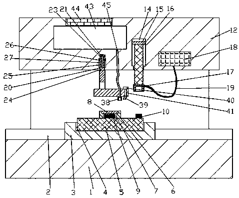
[0013] see Figure 1-3, an embodiment provided by the present invention: a power supply circuit and a semiconductor integrated circuit device, including a fixed base plate 1, the upper end of the fixed base plate 1 is provided with a transmission groove 2 extending left and right, and the transmission groove 2 is set There is a transmission trolley 3, and a fixing groove 4 with an upward opening is arranged at the middle position of the upper end surface of th...


PUM


Abstract

The present invention discloses a power circuit and semiconductor integration circuit device. The device comprises a fixed bottom plate, the upper end of a support plate is fixedly connected with a working housing extended forwards, the lower end of a hydraulic rod passes through the lower end wall of a hydraulic space and is fixedly connected with an interventional device, the right side of the internal portion of the working housing is provided with a detector, a glue spraying head is fixedly arranged at the right side of the lower end face of a movable block, a blow nozzle is fixedly arranged at the right end of the lower end face of the movable block, and a waste collection space with an upward opening is arranged at a corresponding position of the rear side of the upper end face of the fixed bottom plate and an electric clamp. In the operation, unqualified products are not subjected to later processing to ensure the quality of the products, avoid unnecessary process waste, save the cost, save human cost and time with automatic gluing, automatically remove the unqualified products and facilitate mistake prevention in the field processing process.

Description

technical field [0001] The invention relates to the field of integrated circuits, in particular to a power supply circuit and semiconductor integrated circuit equipment. Background technique [0002] An integrated circuit is a microelectronic device or component that uses a certain process to interconnect components such as transistors, resistors, capacitors, and inductors required in a circuit, and interconnects them together to form a small or several small semiconductor chips or chips. Dielectric substrate, and then encapsulated in a package, to become a microstructure with the required circuit function, in which all components have been structurally integrated, making electronic components towards miniaturization, low power consumption, intelligence and high reliability. It has taken a big step forward in terms of safety. In the production process of semiconductor integrated circuits, glue coating and sealing are usually required, and inspection is carried out after the ...

Claims


Application Information

Patent Timeline
Patent Type & Authority Applications(China)
IPC IPC(8): H01L21/67
CPCH01L21/67126
Inventor 吴城杰
Owner NINGBO LINGLI IND PROD DESIGN CO LTD
Why Eureka
Try Eureka