Nonvolatile memory based on two-dimensional ferroelectric semiconductor and its preparation method

A non-volatile memory and two-dimensional semiconductor technology, applied in the direction of electrical components, etc., can solve the problems of restricting the application of ferroelectric memory and low storage density, and achieve high practicability and application value, high crystal quality, and increase storage density. Effect

Active Publication Date: 2021-01-29
ZHEJIANG XINKE SEMICON CO LTD
View PDF3 Cites 0 Cited by
  • Summary
  • Abstract
  • Description
  • Claims
  • Application Information

AI Technical Summary

Problems solved by technology

However, in order to increase the data storage density, it is usually necessary to use the polarization of the ferroelectric film in the vertical direction. When such a ferroelectric material is made into a film by surface epitaxial growth technology, due to the effect of the depolarization field, its ferroelectricity in the Most of them will disappe...

Method used


Image

  • Nonvolatile memory based on two-dimensional ferroelectric semiconductor and its preparation method
  • Nonvolatile memory based on two-dimensional ferroelectric semiconductor and its preparation method
  • Nonvolatile memory based on two-dimensional ferroelectric semiconductor and its preparation method

Examples


preparation example Construction

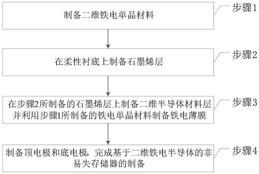
[0051] In an embodiment of the present disclosure, a method for preparing a non-volatile memory based on a two-dimensional ferroelectric semiconductor is provided, which is used to prepare the above-mentioned non-volatile memory, figure 2 It is a schematic flow chart of the preparation method, such as figure 2 Shown, described preparation method comprises:

[0052] Step 1: preparing a two-dimensional ferroelectric single crystal material;

[0053] Step 2: preparing a graphene layer on a flexible substrate;

[0054] Step 3: preparing a two-dimensional semiconductor material layer on the graphene layer prepared in step 2 and using the ferroelectric single crystal material prepared in step 1 to prepare a ferroelectric film; and

[0055] Step 4: Prepare the top electrode and the bottom electrode, and complete the preparation of the nonvolatile memory based on the two-dimensional ferroelectric semiconductor;

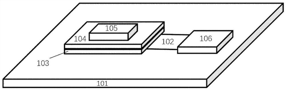
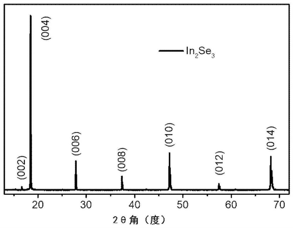
[0056] In said step 1, taking the preparation of two-dimensional fe...


PUM

PropertyMeasurementUnit
Thicknessaaaaaaaaaa
Thicknessaaaaaaaaaa

Abstract

A nonvolatile memory based on a two-dimensional ferroelectric semiconductor, comprising: a substrate made of a flexible material; a graphene layer, elongated, located on the substrate; a two-dimensional semiconductor material layer, located on the substrate a bottom and a part of the graphene layer; a ferroelectric film on the two-dimensional semiconductor material layer; a top electrode on the ferroelectric film; and a bottom electrode on a part of the graphene layer; The preparation method of the volatile memory includes: first preparing a two-dimensional ferroelectric single crystal material; preparing a graphene layer on a flexible substrate; preparing a two-dimensional semiconductor material layer on the prepared graphene layer and using the prepared ferroelectric single crystal crystalline material to prepare ferroelectric thin film; and prepare top electrode and bottom electrode to complete the preparation of non-volatile memory based on two-dimensional ferroelectric semiconductor, so as to alleviate the difficult quantum tunneling and heat dissipation difficulties after further miniaturization of memory in the prior art. technical problem.

Description

technical field [0001] The present disclosure relates to the fields of preparation of two-dimensional semiconductor materials and ferroelectric storage, and in particular to a nonvolatile memory based on two-dimensional ferroelectric semiconductors and a preparation method thereof. Background technique [0002] Non-volatile memory cells are an integral part of digital, portable, self-contained electronics, and are receiving increasing attention due to their miniaturization, low power consumption, and reliable data storage, which are ideally suited to address large data capacity and integration issues. Attention, memory based on ultra-thin two-dimensional materials has been studied and reported, due to its excellent electrical properties and storage density, it has great potential for development, among them, memory devices based on ferroelectric materials have simple storage structure, high storage density, The advantages of low power consumption, high storage speed, radiati...

Claims


Application Information

Patent Timeline
IPC IPC(8): H01L45/00
CPCH10N70/801H10N70/8825H10N70/023H10N70/8828
Inventor 杨淮魏钟鸣李京波
Owner ZHEJIANG XINKE SEMICON CO LTD
Why Eureka
Try Eureka