
Mask plate, manufacturing method of mask plate and forming method of semiconductor device

A manufacturing method and a technology of a mask plate, which are applied in the direction of instruments, photoplate-making process of pattern surface, and originals used for photomechanical processing, etc., can solve the problems that the performance of the mask plate needs to be improved, so as to improve the exposure ability and intensity increased effect

Inactive Publication Date: 2019-01-29
HUAIAN IMAGING DEVICE MFGR CORP
View PDF5 Cites 0 Cited by
  • Summary
  • Abstract
  • Description
  • Claims
  • Application Information

AI Technical Summary

Problems solved by technology

[0004] However, the performance of existing masks needs to be improved

Method used


Image

  • Mask plate, manufacturing method of mask plate and forming method of semiconductor device
  • Mask plate, manufacturing method of mask plate and forming method of semiconductor device
  • Mask plate, manufacturing method of mask plate and forming method of semiconductor device

Examples


Embodiment Construction

[0026] As mentioned in the background, the reticle formed by the prior art has poor performance.

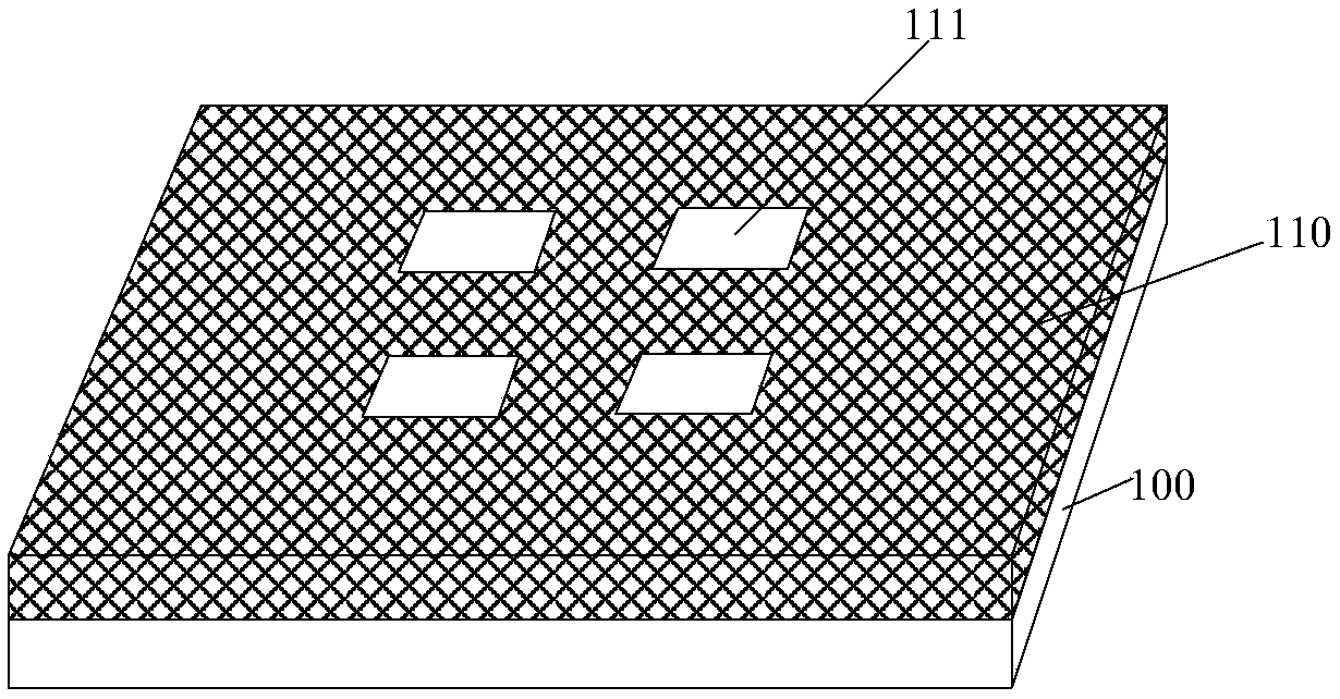
[0027] A mask version, please refer to figure 1 , comprising: a substrate 100; a light blocking layer 110 located on the substrate 100, the light blocking layer 110 has four openings 111 adjacent to each other.

[0028] In the process of exposing the photoresist film on the layer to be etched using the mask plate as a mask, the center of the area surrounded by the four openings 111 will be affected by the diffraction of light at the four openings 111, Therefore, the light intensity at the center of the area surrounded by the four openings 111 is relatively strong. For convenience of description, the center of the area surrounded by the four openings 111 is referred to as the first area. In this way, after the light passes through the mask plate, a pattern will be formed in the photoresist film under the first region. After the photoresist film is developed, holes are formed in...


PUM

PropertyMeasurementUnit
Thicknessaaaaaaaaaa

Abstract

The invention discloses a mask plate, a manufacturing method of the mask plate and a forming method of a semiconductor device. The mask plate comprises a substrate, a light blocking layer located on the substrate, and a phase shifting layer, wherein an opening set is arranged in the light blocking layer, and the opening set comprises a plurality of openings adjacent to each other; the openings runthrough the light blocking layer and are exposed out of the surface of the substrate; a phase shifting notch running through the light blocking layer is further formed in the light blocking layer, and the phase shifting notch is separated from the openings and is surrounded by the openings in the opening set; the phase shifting layer is located on the surface, at the bottom of the phase shiftingnotch, of the substrate. The performance of the mask plate is improved.

Description

technical field [0001] The invention relates to the field of semiconductor manufacturing, in particular to a mask plate, a manufacturing method thereof, and a method for forming a semiconductor device. Background technique [0002] The photomask substrate is an ideal photosensitive blank plate for making fine photomask patterns, and the required mask plate can be obtained through the photolithography process. [0003] Masks are widely used in fields involving photolithography, such as IC (Integrated Circuit, integrated circuit), FPD (Flat Panel Display, flat panel display, PCB (Printed Circuit Boards, printed circuit board, MEMS (Micro Electro Mechanical Systems, Micro Electro Mechanical Systems), etc. [0004] However, the performance of existing masks needs to be improved. Contents of the invention [0005] The problem to be solved by the present invention is to provide a mask plate and its manufacturing method, and a method for forming a semiconductor device, so as to...

Claims


Application Information

Patent Timeline
IPC IPC(8): G03F1/26
CPCG03F1/26
Inventor 侯士权夏睿梁凤云徐一建王婷
Owner HUAIAN IMAGING DEVICE MFGR CORP
Learn More