Display screen, pixel circuit unit and control method thereof
A pixel circuit and pixel technology, applied in static indicators, instruments, etc., can solve the problems of inability to achieve display and PPI stagnation, and achieve the effects of simple wiring, increased grayscale, and simplified Mask process.
- Summary
- Abstract
- Description
- Claims
- Application Information
AI Technical Summary
Problems solved by technology
Method used
Image
Examples
Embodiment 1
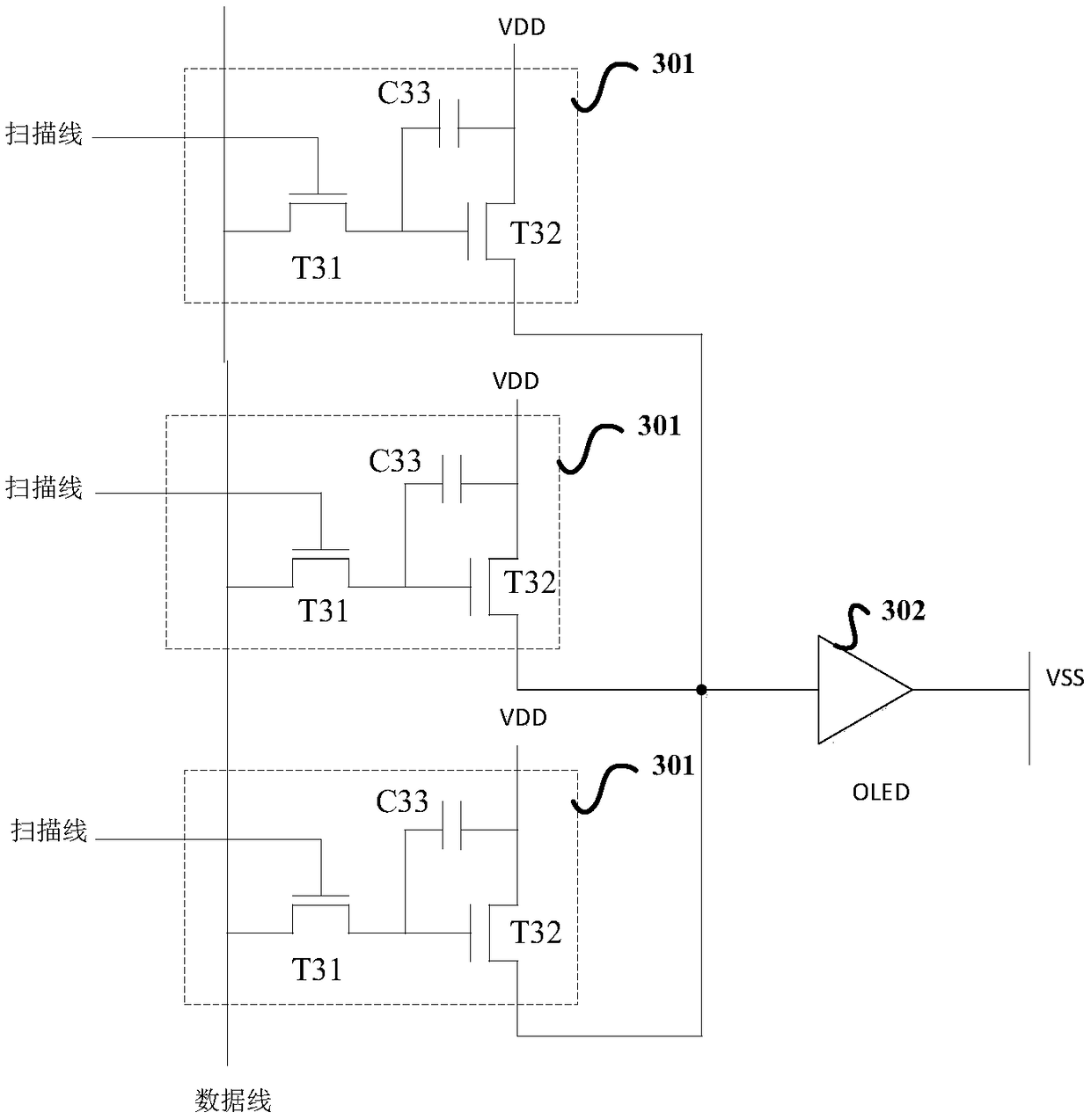
[0048] A circuit diagram of a pixel circuit unit provided by Embodiment 1 of the present invention, as shown in image 3 As shown, it includes: a light emitting device 302 and at least two simple pixel compensation circuits 301 .
[0049] Wherein, there is one light emitting device 302 , and the at least two simple pixel compensation circuits 301 are connected to the light emitting device 302 to provide driving current for the light emitting device 302 .
[0050] Preferably, the simple pixel compensation circuit 301 is specifically a 2T1C circuit, that is, a pixel compensation circuit based on two transistors and one capacitor.
[0051] Preferably, there are three simple pixel compensation circuits 301 . Figure 4 A schematic diagram showing low, medium and high grayscale display of the light emitting device in the pixel circuit unit with three simple pixel compensation circuits 301 is shown.
[0052] In fact, a pixel circuit unit with 3 2T1C circuits can have 64 gray levels...
Embodiment 2
[0056] A circuit diagram of a pixel circuit unit provided in Embodiment 2 of the present invention, as shown in Figure 5 As shown, it includes: a light emitting device 501, and at least two simple pixel compensation circuits 502;
[0057] Wherein, at least two simple pixel compensation circuits 502 are connected to the light emitting device 501 to provide driving current for the light emitting device 501 . Specifically, there are multiple light emitting devices 501, and the number of light emitting devices 501 is the same as the number of the simple pixel compensation circuits 502, and each simple pixel compensation circuit 502 provides driving current for one light emitting device 501 respectively.
[0058] Preferably, the simple pixel compensation circuit 502 is specifically a 2T1C circuit, that is, a pixel compensation circuit based on two transistors and one capacitor.
[0059] Preferably, there are three light emitting devices 501 and three simple pixel compensation cir...
Embodiment 3
[0070] Based on the pixel circuit unit of the first or second embodiment above, the third embodiment of the present invention provides a display screen, such as Figure 8 As shown, it includes: a plurality of pixel circuit units 801 and a control module 802 thereof.
[0071] Wherein, the specific circuit of the pixel circuit unit 801 may be the circuit of the pixel circuit unit of the first embodiment described above, or the circuit of the pixel circuit unit of the second embodiment described above.
[0072] The control module 802 can be set in the signal processing chip and connected to each pixel circuit unit 801: the control module 802 can provide a scan signal for each simple pixel compensation circuit in each pixel circuit unit 801 through the scan line, and the control module 802 can provide a scan signal through the scan line. The data line can provide brightness control voltage V for each simple pixel compensation circuit in each pixel circuit unit 801 data .
[0073] ...
PUM
 Abstract
Description
Claims
Application Information
 - R&D
- Intellectual Property
- Life Sciences
- Materials
- Tech Scout
- Unparalleled Data Quality
- Higher Quality Content
- 60% Fewer Hallucinations
Browse by: Latest US Patents, China's latest patents, Technical Efficacy Thesaurus, Application Domain, Technology Topic, Popular Technical Reports.
© 2025 PatSnap. All rights reserved.Legal|Privacy policy|Modern Slavery Act Transparency Statement|Sitemap|About US| Contact US: help@patsnap.com


