A method for manufacturing a flexible capacitive touch screen
A technology of flexible capacitors and manufacturing methods, applied in the direction of electrical digital data processing, input/output process of data processing, instruments, etc., can solve the problems of process failure, PI film peeling, etc., achieve the effect of reducing thickness and saving production processes
- Summary
- Abstract
- Description
- Claims
- Application Information
AI Technical Summary
Problems solved by technology
Method used
Image
Examples
Embodiment 1
[0038] A method for manufacturing a flexible capacitive touch screen, comprising:
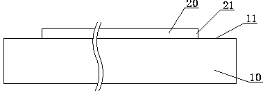
[0039] Step 1, such as figure 1 As shown, the first side of the soda-lime glass substrate 10 is coated with a polyamic acid solution by using the slot coating method, and thermally polymerized into a PI film 20 with a thickness of about 30 μm (5-200 μm is acceptable). The edge 21 of the PI film 20 is On the first surface of the glass substrate, there is a bare area 11 of the glass substrate 10 outside the PI film 20;
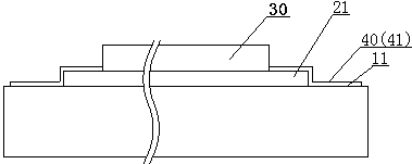
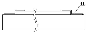
[0040] Step two, such as figure 2 , image 3 As shown, a baffle 30 is placed on the PI film 20 (need to be removed later), only the edge 21 of the PI film is exposed, and the edge 21 of the PI film is sprayed with a fluoropolymer solution and dried and heat-cured to form a layer as A fluoropolymer coating 40 (typically a polytetrafluoroethylene coating) of the barrier layer 41, the fluoropolymer coating 40 spans the edge 21 of the PI film, covering from the bare area 11 to th...
Embodiment 2
[0045] On the basis of the first embodiment, changing the barrier layer 41 to an acid-resistant metal thin film deposited by magnetron sputtering constitutes the second embodiment of the present invention.
[0046] Specifically, the same as figure 2 , image 3 As shown, its step 2 is changed to: place a mask 30 on the PI film 20, only expose the edge 21 of the PI film, adopt magnetron sputtering to deposit a gold acid-resistant film 40 with a thickness of about 100 nm on the first side of the glass substrate 10 (It can also be an acid-resistant metal film such as molybdenum, tungsten, etc.), the acid-resistant film crosses the edge 21 of the PI film, and covers the part of the film body from the exposed area 11 of the glass substrate to the edge 21 of the PI film to form a barrier layer 41 .
[0047] The acid-resistant metal film deposited by magnetron sputtering has very high density, so the barrier layer 41 also has an ideal barrier effect on water.
Embodiment 3
[0049] Such as Figure 7 As shown, on the basis of Embodiment 1, the barrier layer 41 is changed to silicon dioxide (SiO2) deposited by magnetron sputtering. 2 ) film, and the silicon dioxide film is also used as a buffer layer between the touch circuit layer and the PI film, which constitutes the third embodiment of the present invention.
[0050] Specifically, step 2 is changed to: deposit a layer of silicon dioxide (SiO2) on the first surface of the glass substrate 10 by magnetron sputtering. 2 ) film 40.
[0051] Wherein, the thickness of silicon dioxide thin film 40 is about 10nm, and it not only covers the edge of PI film and the exposed place of glass substrate to form barrier layer 41, also covers to other positions of PI film 20, forms the barrier layer 41 between PI film 20. The buffer layer 42 of the touch circuit layer 50 is formed on it, which is beneficial to improve the bonding force between the touch circuit layer 50 and the PI film 20 .
PUM
| Property | Measurement | Unit |
|---|---|---|
| thickness | aaaaa | aaaaa |
| thickness | aaaaa | aaaaa |
| thickness | aaaaa | aaaaa |
Abstract
Description
Claims
Application Information
 - R&D
- Intellectual Property
- Life Sciences
- Materials
- Tech Scout
- Unparalleled Data Quality
- Higher Quality Content
- 60% Fewer Hallucinations
Browse by: Latest US Patents, China's latest patents, Technical Efficacy Thesaurus, Application Domain, Technology Topic, Popular Technical Reports.
© 2025 PatSnap. All rights reserved.Legal|Privacy policy|Modern Slavery Act Transparency Statement|Sitemap|About US| Contact US: help@patsnap.com


