Organic electroluminescent device and its preparation method
An electroluminescent device and electroluminescent technology, which can be applied to organic light-emitting devices, organic semiconductor devices, electric solid-state devices, etc., and can solve problems such as lifespan decline.
- Summary
- Abstract
- Description
- Claims
- Application Information
AI Technical Summary
Problems solved by technology
Method used
Image
Examples
Embodiment approach 1
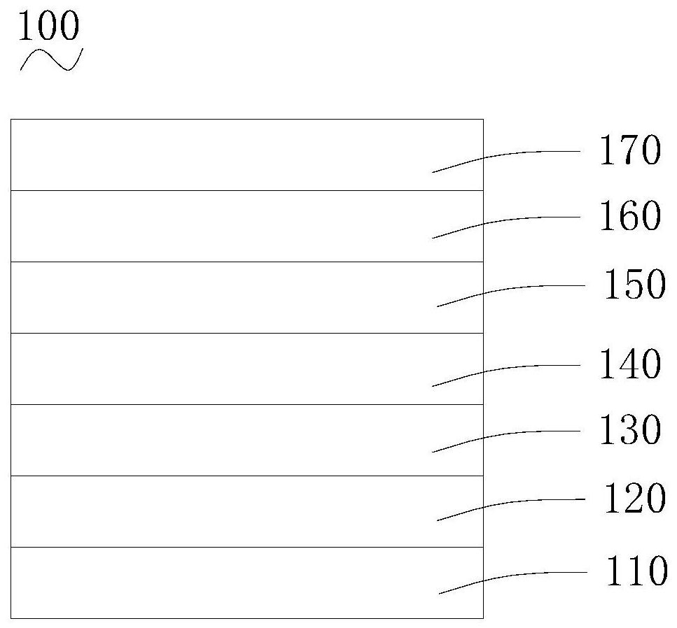
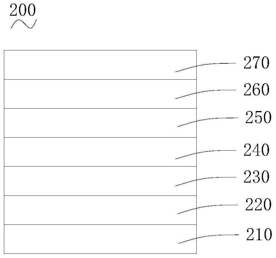
[0043] The organic electroluminescent device of Embodiment 1 includes an anode and a hole injection layer, a hole transport layer, an electron blocking layer, an organic light emitting layer, an electron transport layer and a cathode formed sequentially on the anode.
[0044] Wherein, the hole injection layer includes a first doped layer. The first doped layer includes P-type dopants. The P-type dopant can increase the amount of hole injection, thereby increasing the lifetime of mass-produced devices.
[0045] On the basis of the foregoing embodiments, the hole injection layer is composed of the first doped layer. The first doped layer is composed of P-type dopants. At this time, only the P-type dopant is contained in the first doped layer, which is more conducive to increasing the injection amount of holes, thereby improving the lifespan of mass-produced devices. It should be noted that, the P-type dopant in this embodiment may contain a small amount of impurities within t...
Embodiment approach 2
[0073] The difference between the organic electroluminescent device of the second embodiment and the organic electroluminescent device of the first embodiment is that the hole injection layer includes a second doped layer. The second doped layer includes a P-type dopant and a hole transport material. By adjusting the doping concentration of the P-type dopant, the injection amount of holes can be controlled, thereby adjusting the balance of electrons and holes, thereby improving the lifespan of mass-produced devices.
[0074] On the basis of the foregoing embodiments, the hole injection layer is composed of the second doped layer. The second doped layer consists of P-type dopants and hole transport material. At this time, the second doped layer only contains P-type dopants and hole transport materials, which is more conducive to controlling the injection of holes, thereby adjusting the balance of electrons and holes, thereby improving the life of mass-produced devices . It s...
Embodiment approach 3
[0091] The difference between the organic electroluminescent device of Embodiment 3 and the organic electroluminescent devices of Embodiment 1 and Embodiment 2 is that the hole injection layer includes a first doped layer and a second doped layer formed on the first doped layer. a doped layer, the second doped layer is close to the hole transport layer.
[0092] On the basis of the foregoing embodiments, the thickness of the first doped layer is 1 nm˜10 nm, and the thickness of the second doped layer is 10 nm˜20 nm.
[0093] The organic electroluminescent device of Embodiment 3 can adjust the injection amount of holes, and at the same time improve the efficiency and lifetime of the device. The difference between the organic electroluminescent device of the fourth embodiment and the organic electroluminescent device of the third embodiment is that the hole injection layer includes a second doped layer and a first doped layer formed on the second doped layer, and the second dope...
PUM
| Property | Measurement | Unit |
|---|---|---|
| thickness | aaaaa | aaaaa |
| thickness | aaaaa | aaaaa |
| thickness | aaaaa | aaaaa |
Abstract
Description
Claims
Application Information
 - R&D
- Intellectual Property
- Life Sciences
- Materials
- Tech Scout
- Unparalleled Data Quality
- Higher Quality Content
- 60% Fewer Hallucinations
Browse by: Latest US Patents, China's latest patents, Technical Efficacy Thesaurus, Application Domain, Technology Topic, Popular Technical Reports.
© 2025 PatSnap. All rights reserved.Legal|Privacy policy|Modern Slavery Act Transparency Statement|Sitemap|About US| Contact US: help@patsnap.com


