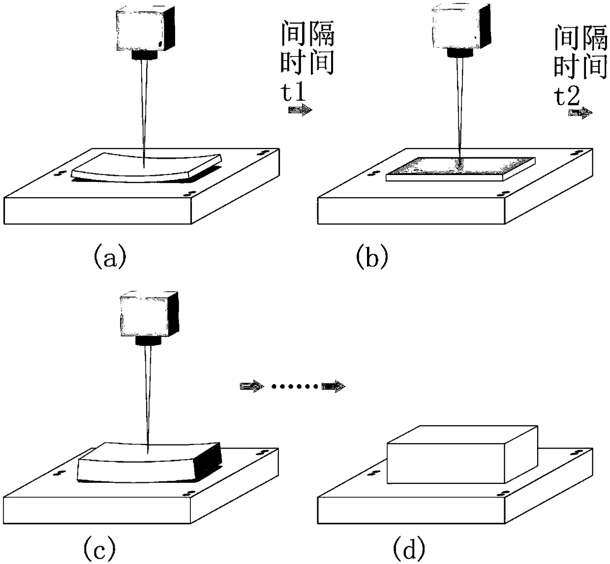
Added material manufacturing method for synchronous heat treatment
A kind of additive manufacturing and laser technology, applied in the field of additive manufacturing, can solve the problems of increasing ceramic phase or alloy element burning loss, low efficiency, large energy loss, etc., and achieve the effect of reducing stress, cooling speed and ensuring performance
- Summary
- Abstract
- Description
- Claims
- Application Information
AI Technical Summary
Problems solved by technology
Method used
Image
Examples
Embodiment 1
[0032]In this embodiment, AlSi10Mg / Al is formed 2 o 3 Composite materials are taken as an example for illustration, which includes the following steps:
[0033] S1 Laying of AlSi with a thickness of 20 μm 10 Mg / Al 2 o 3 Composite powder, the powder spreading time is 10s, the powder is melted and formed with 200W laser power, 200mm / s scanning speed, and 0.12mm scanning distance, and the scanning process of one layer is completed. Due to the large temperature gradient and internal stress in the forming process , will cause slight stress deformation of the entity, and even edge cracking;
[0034] After an interval of 1s in S2, reheat the completed layer with 100W laser power, 1200mm / s scanning speed, and 0.12mm scanning distance to play the role of post-heating to reduce the cooling rate when SLM forming cermet materials, but not melt formed layers;
[0035] S3 Repeating steps S1 and S2, the edge of the final formed solid will not be cracked due to stress, and a dense part ...
Embodiment 2
[0037] This embodiment takes the forming of AlSi10Mg / SiC material as an example for illustration, which includes the following steps:
[0038] S1 lays AlSi10Mg / SiC composite powder with a thickness of 40μm, and the powder laying time is 5s. The powder is melted and formed with 2000W laser power, 3000mm / s scanning speed, and 0.08mm scanning distance to complete the scanning process of one layer. There is a large temperature gradient and internal stress, which will cause slight stress deformation of the entity, and even edge cracking;
[0039] After an interval of 0.2s in S2, reheat the completed layer with 200W laser power, 2000mm / s scanning speed, and 0.12mm scanning distance to play the role of afterheating and reduce the cooling rate when SLM forms cermet materials, but does not melt formed layers;
[0040] S3 Repeating steps S1 and S2, the edge of the final formed solid will not be cracked due to stress, and a dense part with good shape and quality can be obtained, and the...
Embodiment 3
[0042] This embodiment takes forming IN718 superalloy material as an example for illustration, which includes the following steps:
[0043] S1 lays metal powder with a thickness of 30μm, and the powder laying time is 8s. The powder is melted and formed with 390W laser power, 1000mm / s scanning speed, and 0.1mm scanning distance to complete the scanning process of one layer. The temperature gradient and internal stress will cause the entity to have slight stress deformation and even edge cracking;
[0044] S2: After an interval of 0.5s, reheat the completed layer with 100W laser power, 3000mm / s scanning speed, and 0.1mm scanning distance to play the role of afterheating, but do not melt the formed layer;
[0045] S3 repeating steps S1 and S2, finally forming a dense part with no cracks on the edge of the solid body and good shape and quality, and the density reaches more than 99.9%.
PUM
| Property | Measurement | Unit |
|---|---|---|
| Thickness | aaaaa | aaaaa |
Abstract
Description
Claims
Application Information
 - R&D
- Intellectual Property
- Life Sciences
- Materials
- Tech Scout
- Unparalleled Data Quality
- Higher Quality Content
- 60% Fewer Hallucinations
Browse by: Latest US Patents, China's latest patents, Technical Efficacy Thesaurus, Application Domain, Technology Topic, Popular Technical Reports.
© 2025 PatSnap. All rights reserved.Legal|Privacy policy|Modern Slavery Act Transparency Statement|Sitemap|About US| Contact US: help@patsnap.com

