Precise depth-controlled groove milling-based manufacture method of microwave printed circuit board

A technology of printed circuit boards and manufacturing methods, which is applied in the direction of printed circuit manufacturing, printed circuits, electrical components, etc., can solve the problems of low production efficiency, inability to do it accurately, and inability to control the tolerance of PCB boards well, so as to ensure zero Residue, the effect of ensuring signal integrity

Inactive Publication Date: 2019-01-01
SHENZHEN SUNTAK MULTILAYER PCB
View PDF3 Cites 3 Cited by
  • Summary
  • Abstract
  • Description
  • Claims
  • Application Information

AI Technical Summary

Problems solved by technology

[0003] In the prior art, stepped grooves are usually made by forming gongs and boards, and using methods such as pressing covering films. This method has the following disadvantages: it is made by forming gongs and boards, and it is impossible to accurately ensure that the next layer of foundation will not be damaged after slotting. The material or the slotting did not reach the target substrate layer, and at the same time, the tolerance of the PCB board cannot be well controlled; and the PCB board will be thickened during the production process by using methods such as pressing the cover film, resulting in the risk that the thickness of the PCB board exceeds the tolerance. Does not meet product production standards, and this production method is cumbersome and has low production efficiency

Method used


Image

  • Precise depth-controlled groove milling-based manufacture method of microwave printed circuit board
  • Precise depth-controlled groove milling-based manufacture method of microwave printed circuit board
  • Precise depth-controlled groove milling-based manufacture method of microwave printed circuit board

Examples


Embodiment

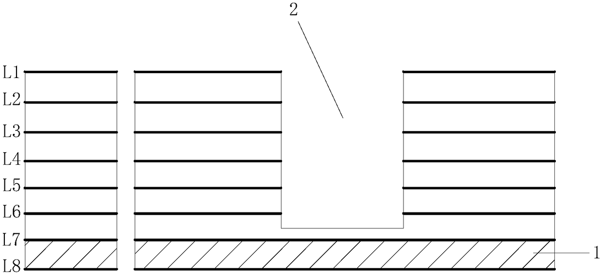
[0029] This embodiment provides a method for manufacturing a circuit board, including a method for manufacturing a microwave printed circuit board with precisely controlled depth milling grooves. The specific process is as follows:

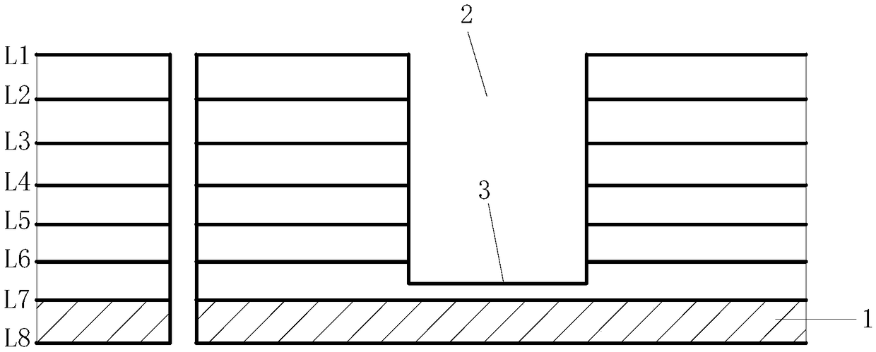
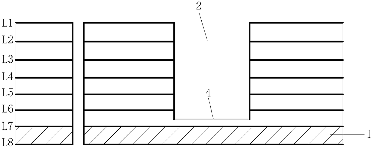
[0030] (1) Cutting: Cut out four core boards according to the board size 520mm×620mm, such as figure 1 As shown, the four core boards are the L1-L2 layer, L3-L4 layer, L5-L6 layer, and L7-L8 layer in the figure, and the dielectric layer of the L7-L8 layer core board is Rogers high-frequency board.

[0031] (2), inner layer circuit making (negative film process): inner layer graphics transfer, coating photosensitive film on the core board with a vertical coating machine, the film thickness of the photosensitive film is controlled at 8 μm, and a fully automatic exposure machine is used to 5-6 Grid exposure ruler (21 grid exposure ruler) completes the exposure of the inner layer circuit on the core board; inner layer etching, etches the inner layer c...


PUM


Abstract

The invention discloses a precise depth-controlled groove milling-based manufacture method of a microwave printed circuit board. The method includes the following steps that: a stepped groove is formed in a production board by means of depth-controlled groove milling, and the groove bottom of the stepped groove is located in a dielectric layer at the upper part of a copper layer at the inner sideof a Rogers high-frequency board; electroless copper plating and full-board electroplating treatment are performed on the production board, so that the groove bottom and groove wall of the stepped groove are plated with a copper layer; the production board is coated with a film, and an outer layer pattern is formed on the production board by means of explosion and development, pattern plating is performed on the production board; a plated layer at the bottom of the stepped groove is removed by means of milling, so that the dielectric layer at the bottom of the stepped groove is exposed; the dielectric layer at the bottom of the stepped groove is burned through laser, so that the copper layer at the inner side of the Rogers high-frequency board is exposed; and adhesive removing treatment isperformed on the production board, and the copper layer exposed at the bottom of the stepped groove is removed by means of alkaline etching. With the method of the invention adopted, the zero damageof the Rogers high-frequency board is realized, and the signal integrity of a high-frequency and high-speed printed circuit board during signal transmission can be ensured.

Description

technical field [0001] The invention relates to the technical field of printed circuit board manufacturing, in particular to a method for manufacturing a microwave printed circuit board with precisely controlled depth milling grooves. Background technique [0002] With the advancement of science and technology, electronic products have become indispensable daily necessities in people's lives, and printed circuit boards (PCB for short) are an important part of electronic products. In recent years, people have more and more functional requirements for electronic products. There are more and more, which puts higher requirements on the PCB. Usually, in order to facilitate the installation of special-function devices or devices that need to be sunken on the PCB, it is often necessary to set up stepped grooves on the PCB. The stepped grooves are also used to achieve high-power products. An important part of heat dissipation, widely used in the industry. [0003] In the prior art,...

Claims


Application Information

Patent Timeline
Patent Type & Authority Applications(China)
IPC IPC(8): H05K3/00H05K3/18
CPCH05K3/0044H05K3/18H05K2203/0228H05K2203/107
Inventor 宋建远彭卫红张盼盼孙保玉
Owner SHENZHEN SUNTAK MULTILAYER PCB
Why Eureka
Try Eureka