LED array interface circuit with energy storage link
A technology of LED array and interface circuit, which is applied in the field of DC-DC conversion interface circuit, can solve the problems of increasing input current ripple and achieve the effect of simple circuit structure
- Summary
- Abstract
- Description
- Claims
- Application Information
AI Technical Summary
Problems solved by technology
Method used
Image

Examples
Embodiment 1
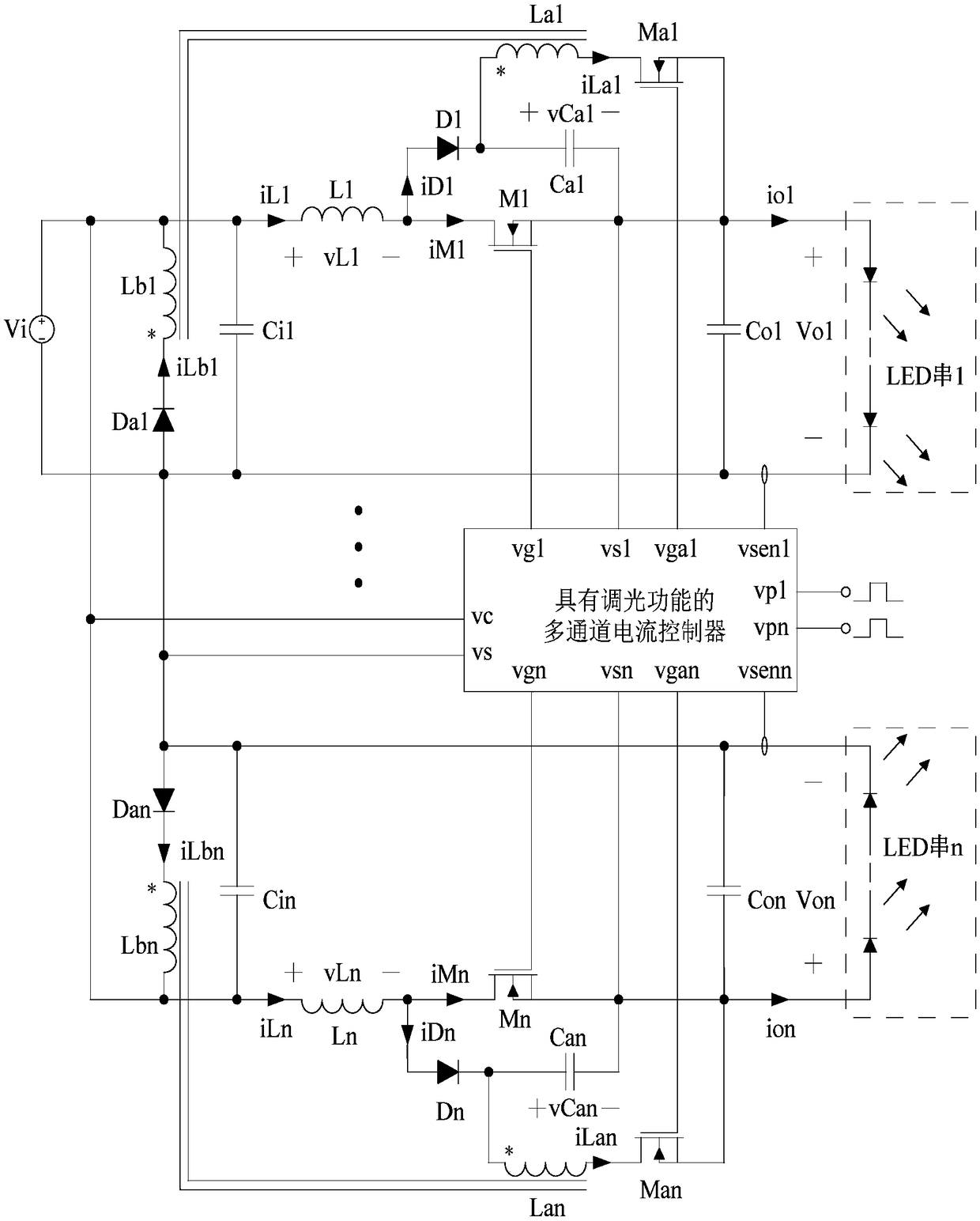
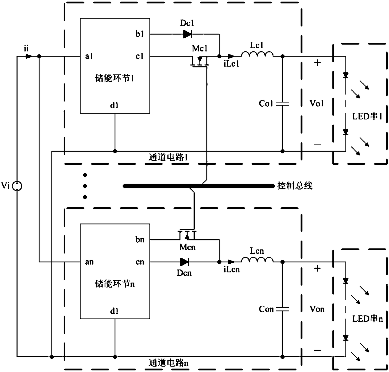
[0020] refer to figure 2 , image 3 and Figure 5 , the LED array interface circuit including the energy storage link includes channel circuit 1 to channel circuit n and a group of control buses. The channel circuit j includes an energy storage link j, a diode Dcj, an N-type MOS transistor Mcj, an inductor Lcj and a capacitor Coj, and the value of j ranges from 1 to n. The energy storage link j has a port aj, a port bj, a port cj and a port dj, the port aj is connected to the positive terminal of the DC power supply Vi, the port bj is connected to the anode of the diode Dcj, and the port cj is connected to the drain of the N-type MOS transistor Mcj, Port dj is connected to the negative terminal of DC power Vi. The cathode of the diode Dcj is simultaneously connected to the source of the N-type MOS transistor Mcj and one end of the inductor Lcj, the other end of the inductor Lcj is simultaneously connected to one end of the capacitor Coj and the anode of the LED string j, a...
Embodiment 2
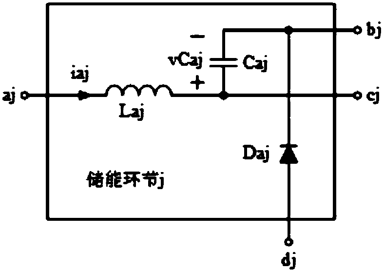
[0027] refer to figure 2 , Figure 4 and Figure 6 , the energy storage link j in the LED array interface circuit including the energy storage link includes an inductor Lbj, a capacitor Cbj and a diode Dbj, one end of the capacitor Cbj is connected to the port aj and port cj of the energy storage link j at the same time, and the other end of the capacitor Cbj is simultaneously One end of the inductor Lbj is connected to the port bj of the energy storage link j, the other end of the inductor Lbj is connected to the cathode of the diode Dbj, and the anode of the diode Dbj is connected to the port dj of the energy storage link j.
[0028] Other circuit structures of the second embodiment are the same as those of the first embodiment.
[0029] When channel circuit j is in continuous conduction mode, its steady-state working process includes the following two stages.
[0030] Stage 1: N-type MOS transistor Mcj is cut off, diode Dcj is turned on, diode Dbj is turned on, DC power...
PUM
 Abstract
Description
Claims
Application Information
 - R&D Engineer
- R&D Manager
- IP Professional
- Industry Leading Data Capabilities
- Powerful AI technology
- Patent DNA Extraction
Browse by: Latest US Patents, China's latest patents, Technical Efficacy Thesaurus, Application Domain, Technology Topic.
© 2024 PatSnap. All rights reserved.Legal|Privacy policy|Modern Slavery Act Transparency Statement|Sitemap