Silicon carbide trench type MOSFETs integrated with SBD and preparation method thereof

A silicon carbide trench and silicon carbide substrate technology, which is applied in semiconductor/solid-state device manufacturing, electrical components, circuits, etc., can solve problems such as excessive electric field, achieve small Le charge, reduce overlapping area, and improve carrier migration rate effect

Active Publication Date: 2018-12-07
INST OF SEMICONDUCTORS - CHINESE ACAD OF SCI
View PDF5 Cites 10 Cited by
  • Summary
  • Abstract
  • Description
  • Claims
  • Application Information

AI Technical Summary

Problems solved by technology

[0005] The purpose of the present invention is to provide a silicon carbide trench MOSFETs integrated with SBDs, so as to alleviate the problem of excessive electric field of the gate dielectric in silicon carbide trench MOSFETs in the prior art, and at the same time greatly improve the power source when MOSFETs work in reverse. Leakage current density can effectively suppress the electrical stress of parasitic PN diodes inside SiC trench MOSFETs, thereby improving chip integration and functionality, reducing the total chip area of ​​SiC MOSFETs and SBDs and the cost of the entire power module

Method used


Image

  • Silicon carbide trench type MOSFETs integrated with SBD and preparation method thereof
  • Silicon carbide trench type MOSFETs integrated with SBD and preparation method thereof
  • Silicon carbide trench type MOSFETs integrated with SBD and preparation method thereof

Examples


preparation example Construction

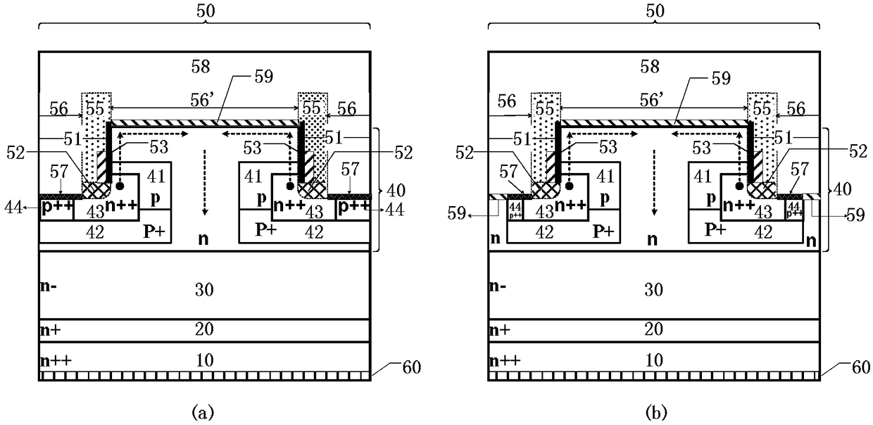
[0109] figure 2 It is a schematic diagram of the steps of the preparation method, such as figure 2 Shown, described preparation method comprises:

[0110] Step A: making a silicon carbide epitaxial wafer substrate; including, sequentially growing an n+ type buffer layer 20, an n-drift layer 30 and an n-type current transport layer 40 on an n++ type silicon carbide substrate 10 from bottom to top, as image 3 shown;

[0111] Step B: Doping the active region in the n-type current transport layer 40, including:

[0112] method 1)

[0113] Sub-step B1: Deposit an implantation mask on the n-type current transport layer 40, pattern it by photolithography, and use doping methods such as ion implantation to form a top-down p-type trench in the n-type current transport layer 40 channel layer 41 and p+ type shielding layer 42, such as Figure 4 shown;

[0114] In the sub-step B1, the doping concentration range of the p-type channel layer 41 is 1×10 16 cm -3 ~1×10 18 cm -3 , ...


PUM

PropertyMeasurementUnit
Thicknessaaaaaaaaaa

Abstract

The invention provides a silicon carbide trench type MOSFETs integrated with an SBD and a preparation method thereof. A side wall gate electrode contact of the MOSFETs is located on the side wall of amain trench, a source electrode metal contact is formed at the bottom of the trench, and a Schottky metal contact is integrated. When a first quadrant is conducted forward, electrons flow from bottomto top through an inversion layer of the side wall of the trench, and a reverse conduction channel different from a conventional trench MOSFETs is formed. When a third quadrant is conducted forward,a Schottky diode is conducted at first, effectively inhibiting conduction of an in-vivo parasitic PN diode. During reverse blocking, a p-type shield layer at the bottom of the trench effectively shields a high electric field in a device body region, so that a device gate dielectric electric field and a Schottky contact electric field are greatly reduced, and an avalanche occurs at a PN junction ofthe device body region. The silicon carbide trench type MOSFETs integrated with an SBD has a low total chip area, satisfies good first and third quadrant conduction characteristics and reverse blocking abilities, and enables the static and dynamic reliability of a device to be improved.

Description

technical field [0001] The invention relates to a structure of a trench type metal-oxide-semiconductor field-effect transistor (MOSFETs) integrating a silicon carbide Schottky diode (SBD) and a preparation method thereof. Background technique [0002] In the field of power electronic conversion, reducing the loss of power devices and the area of ​​integrated chips can significantly improve the overall efficiency of the system. The critical breakdown electric field of silicon carbide is 10 times that of Si, and it is currently the most mature wide bandgap power semiconductor device. SiC trench MOSFETs have higher cell integration and non-polar surface carrier mobility, which can further reduce the chip area and on-state resistance of SiC-based power devices. This makes SiC trench MOSFETs attract more and more attention, especially for power electronics applications such as electric vehicles, charging piles, uninterruptible power supplies and smart grids. [0003] However, w...

Claims


Application Information

Patent Timeline
IPC IPC(8): H01L29/06H01L29/423H01L29/45H01L29/78H01L21/336H01L21/28
CPCH01L29/0684H01L29/401H01L29/4236H01L29/42364H01L29/45H01L29/66068H01L29/7827
Inventor 申占伟张峰温正欣赵万顺王雷闫果果刘兴昉孙国胜曾一平
Owner INST OF SEMICONDUCTORS - CHINESE ACAD OF SCI
Why Eureka
Try Eureka