Broadband reflective half-wave plate based on silicon nano brick array and preparation method of broadband reflective half-wave plate

A silicon nano-brick and half-wave plate technology, applied in the fields of micro-nano optics and polarized optics, can solve the problems of phase delay of polarized light, complicated manufacturing process, large volume and weight, etc., and achieves low weight, simple processing and low cost. Effect

Inactive Publication Date: 2018-11-27
WUHAN POST & TELECOMM RES INST CO LTD
View PDF5 Cites 10 Cited by
  • Summary
  • Abstract
  • Description
  • Claims
  • Application Information

AI Technical Summary

Problems solved by technology

[0004] However, the traditional half-wave plate has many disadvantages: the traditional half-wave plate can only work for one wavelength, and only produces phase delay for incident light of a specific wavelength, large volume and weight, complex manufacturing process, etc.
[0005] In recent years, new half-wave plates based on metasurface materials can manipulate electromagnetic fields in a small wavelength range. However, this new half-wave plate does not solve the problem of only producing phase retardation for a single wavelength of polarized light.

Method used


Image

  • Broadband reflective half-wave plate based on silicon nano brick array and preparation method of broadband reflective half-wave plate
  • Broadband reflective half-wave plate based on silicon nano brick array and preparation method of broadband reflective half-wave plate
  • Broadband reflective half-wave plate based on silicon nano brick array and preparation method of broadband reflective half-wave plate

Examples


Embodiment Construction

[0031] The present invention will be further described in detail below in conjunction with the accompanying drawings and specific embodiments.

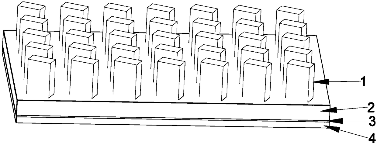
[0032] see figure 1 As shown, the embodiment of the present invention provides a broadband reflective half-wave plate based on a silicon nanobrick array, which includes a substrate 4, a metal reflective layer 3, a dielectric film layer 2 and a silicon nanobrick array arranged from bottom to top 1, wherein the silicon nanobrick array 1 is composed of silicon nanobricks arranged periodically in the same direction and size.

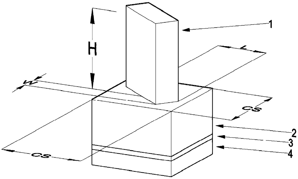
[0033] see figure 2 As shown, the silicon nanobrick is in the shape of a cuboid, and its length, width, and height are both subwavelength dimensions. L is the long axis dimension of the silicon nanobrick, W is the short axis dimension of the silicon nanobrick, H is the height of the silicon nanobrick, and CS is the period of silicon nanobrick array 1.

[0034] Preferably, the substrate 4 is made of glass materia...


PUM

PropertyMeasurementUnit
Bandwidthaaaaaaaaaa

Abstract

The invention discloses a broadband reflective half-wave plate based on a silicon nano brick array and a preparation method of the broadband reflective half-wave plate, and relates to the field of micro-nano optics and polarization optics. The half-wave plate comprises a base, a metal reflection layer, a dielectric medium film layer and a silicon nano brick array arranged from bottom to top, wherein the silicon nano brick array is formed by periodically arranging silicon nano bricks with the same turning direction and size; the structural parameters of the half-wave plate are optimized so thatthe component of the reflected light of the half-wave plate generates a phase delay of Pi in the major-minor axis direction after the linearly polarized light at the communication wave band of optical fiber comes in, and the polarization direction of the incident light is changed. According to the broadband reflective half-wave plate disclosed by the invention, for a light wave with wavelength of1,400-1,700nm, a phase delay of Pi can be generated in the major-minor axis direction of the reflected light.

Description

technical field [0001] The invention relates to the fields of micro-nano optics and polarization optics, in particular to a broadband reflective half-wave plate based on a silicon nano-brick array and a preparation method thereof. Background technique [0002] The traditional half-wave plate (half-wave plate) uses the anisotropy of the transparent crystal to make the incident line polarized light emerge from the crystal, and produce a phase delay of π between the components in the long and short axis directions, thereby changing the polarization of the light state. The half-wave plate is a retardation plate that produces a half-wavelength optical path difference or a 180° phase difference between the phases of the ordinary light and the extraordinary light components of polarized light. [0003] The half-wave plate can rotate the polarized light, because the linearly polarized light is perpendicular to the half-wave plate, and the transmitted light is still linearly polariz...

Claims


Application Information

Patent Timeline
IPC IPC(8): G02B5/30
CPCG02B5/3083
Inventor 郑国兴陶金李嘉鑫武霖刘子晨尤全
Owner WUHAN POST & TELECOMM RES INST CO LTD
Why Eureka
Try Eureka