Schottky junction conduction-type metal oxide semiconductor field effect transistor
A technology of oxide semiconductor and Schottky junction, applied in semiconductor devices, electrical components, circuits, etc., can solve the problems of low channel carrier mobility, long reverse recovery time of devices, and difficulty in reducing on-resistance , to achieve the effects of fast extraction speed, low characteristic on-resistance, and short reverse recovery time
- Summary
- Abstract
- Description
- Claims
- Application Information
AI Technical Summary
Problems solved by technology
Method used
Image
Examples
Embodiment 1
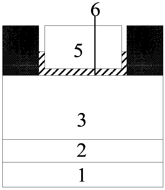
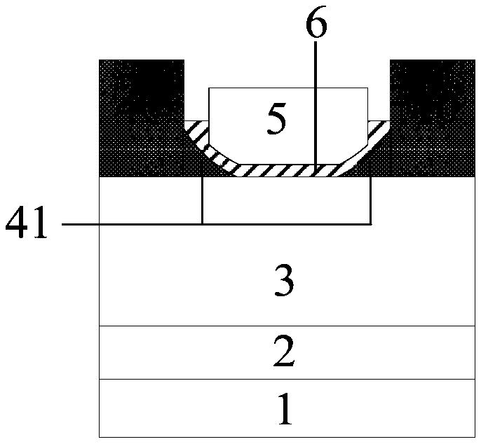
[0028] The invention discloses a Schottky junction conduction metal oxide semiconductor field effect transistor, such as figure 1 As shown, it includes: a drain metal 1, a semiconductor substrate 2 with a high doping concentration is connected above the drain metal 1, a drift region 3 is arranged above the semiconductor substrate 2 with a high doping concentration, and a gate is arranged on the surface of the drift region 3. The oxide layer 6 and the source metal 40, the gate electrode 5 is arranged above the gate oxide layer 6, and the contact between the source metal 40 and the drift region 3 is a Schottky contact.
[0029] When the potential difference between the gate electrode and the source metal is less than or equal to zero, the device is in the off state, and the device uses the Schottky junction between the drift region and the source metal to withstand voltage; when the gate electrode and the source metal When the potential difference is greater than zero, the gate ...
Embodiment 2
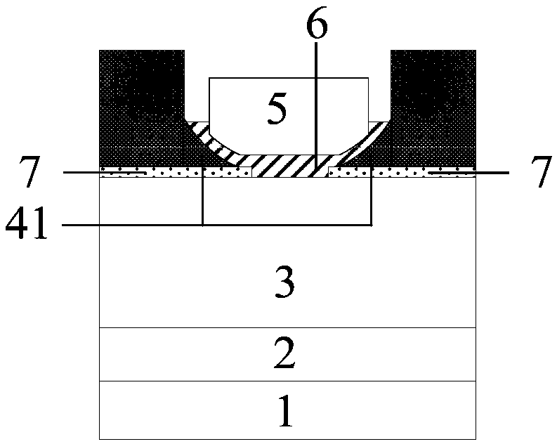
[0038] Such as image 3 As shown, the structure of this embodiment is based on Embodiment 1, adding a layer of Schottky metal layer 7 on the surface of drift region 3, and a good Schottky layer is formed between Schottky metal layer 7 and drift region 3. touch. The structure can adjust the height of the Schottky junction barrier by selecting the material of the Schottky metal layer 7, the height of the Schottky junction barrier can increase the withstand voltage of the device, and the reduction of the barrier height can reduce the device For the turn-on voltage of the body diode, after adding the Schottky metal layer 7, the height of the Schottky junction barrier can be adjusted according to different application requirements, so as to meet actual application requirements.
[0039] It should be noted, image 3 The length of the Schottky metal layer 7 in contact with the drift region 3 in the length direction is greater than the contact length of the source metal 40 with the ...
Embodiment 3
[0042] This embodiment further discloses specific applications of Schottky junction conduction metal oxide semiconductor field effect transistors, such as:
[0043] Schottky junction conduction metal oxide semiconductor field effect transistors can be applied to driver chips of printers, motors or flat panel displays to reduce the characteristic on-resistance and body diode reverse recovery time.
[0044] Schottky junction conduction metal oxide semiconductor field effect transistors can also be applied to power management systems containing field effect transistors to reduce characteristic on-resistance and body diode reverse recovery time.
PUM
 Abstract
Description
Claims
Application Information
 - R&D
- Intellectual Property
- Life Sciences
- Materials
- Tech Scout
- Unparalleled Data Quality
- Higher Quality Content
- 60% Fewer Hallucinations
Browse by: Latest US Patents, China's latest patents, Technical Efficacy Thesaurus, Application Domain, Technology Topic, Popular Technical Reports.
© 2025 PatSnap. All rights reserved.Legal|Privacy policy|Modern Slavery Act Transparency Statement|Sitemap|About US| Contact US: help@patsnap.com


