Optothermal detector and preparation method thereof
A detector and photothermal technology, applied in the field of detectors, can solve the problems of low absorption rate of incident light and achieve the effects of easy preparation, simple structure and high energy conversion efficiency
- Summary
- Abstract
- Description
- Claims
- Application Information
AI Technical Summary
Problems solved by technology
Method used
Image

Examples
Embodiment 1
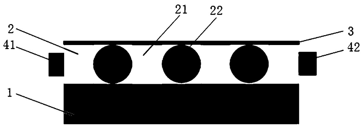
[0034] Such as figure 1 As shown, it is a schematic structural diagram of a photothermal detector according to the embodiment of the present application. The photothermal detector of this embodiment is composed of a base layer, a dielectric layer 1, a first nanolayer 2 and a second nanolayer 3 connected sequentially from bottom to top , the first nano-layer 2 is composed of pyroelectric blocks 21 and metal balls 22 connected alternately, starting with the pyroelectric blocks 21 and ending with the pyroelectric blocks 21, the pyroelectric blocks 21 on both sides of the first nano-layer 2 A first electrode 41 and a second electrode 42 are respectively provided for connecting to an external circuit.
[0035] Specifically: the second nanometer layer 3 is a graphene film layer, and the metal balls 22 are made of noble metal materials. The dielectric layer 1 is made of silicon dioxide, the graphene film layer is two layers of graphene, the thickness of the pyroelectric block 21 is ...
Embodiment 2
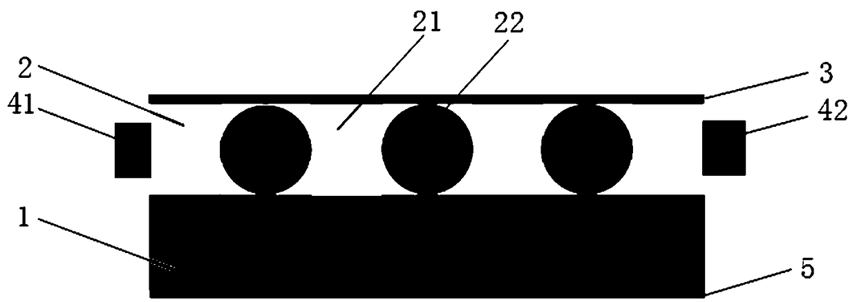
[0044] Such as figure 2 As shown, based on the photothermal detector disclosed in Embodiment 1, the embodiment of the present application discloses a photothermal detector. On the basis of the photothermal detector disclosed in Embodiment 1, the dielectric layer of this embodiment 1. A third nanometer layer 5 is provided on the lower surface, and the third nanometer layer 5 is made of gold material.
[0045] in particular:
[0046] The lower surface of the dielectric layer 1 is further provided with a third nanometer layer 5 made of gold material, and the thickness of the third nanometer layer 5 is 10-200nm. The coupling effect between the gold film and the incident light is used to enhance the absorption of the incident light, so that the light absorption effect of the detector of the embodiment of the present application is better.
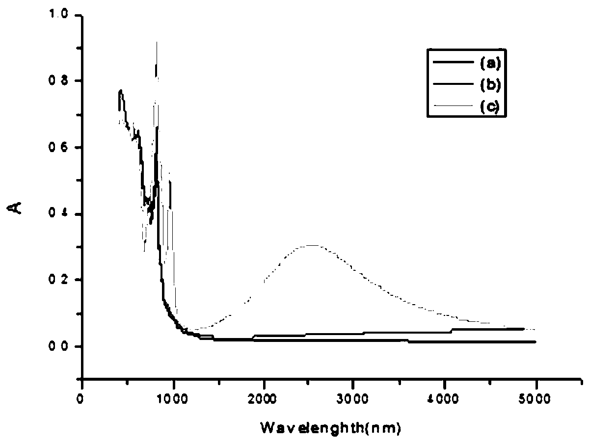
[0047] Such as image 3 As shown in (c), it is the photothermal detector of this embodiment after adding the third nanometer layer 5. The...
Embodiment 3
[0049] Based on the photothermal detector disclosed in Example 1, the embodiment of the present application discloses a method for preparing a photothermal detector, including the following steps:
[0050] Step 1. Prepare the substrate: prepare a clean ITO glass as the substrate layer;
[0051] Step 2, evaporating the dielectric layer: using the electron beam evaporation method to vapor-deposit silicon dioxide on the ITO glass prepared in step 1 to form a dielectric layer;
[0052] Step 3, Glue removal: Use a glue removal machine to coat PMMA photoresist on the dielectric layer formed in step 2, the thickness is the set height of the pyroelectric block, and place the substrate on a hot plate to dry after the glue coating is completed ;
[0053] Step 4, exposure: design the first nano-layer pattern with a pattern generator, and expose the shape of the pyroelectric block with an electron beam to obtain the exposed substrate;
[0054] Step 5, development and fixation: put the s...
PUM
 Abstract
Description
Claims
Application Information
 - R&D
- Intellectual Property
- Life Sciences
- Materials
- Tech Scout
- Unparalleled Data Quality
- Higher Quality Content
- 60% Fewer Hallucinations
Browse by: Latest US Patents, China's latest patents, Technical Efficacy Thesaurus, Application Domain, Technology Topic, Popular Technical Reports.
© 2025 PatSnap. All rights reserved.Legal|Privacy policy|Modern Slavery Act Transparency Statement|Sitemap|About US| Contact US: help@patsnap.com