Solid-state zinc-expanding method of GaAs-based epitaxial wafer

An epitaxial wafer, solid-state technology, used in semiconductor/solid-state device manufacturing, electrical components, circuits, etc., can solve problems such as batch repeatability cannot be fully guaranteed, difficult to grow ZnO at low temperature, etc., to achieve uniformity and consistency of diffusion , good repeatability and consistency, good temperature uniformity

Inactive Publication Date: 2018-11-23
潍坊华光光电子有限公司
View PDF10 Cites 0 Cited by
  • Summary
  • Abstract
  • Description
  • Claims
  • Application Information

AI Technical Summary

Problems solved by technology

Both of the above two methods use MOCVD to grow ZnO as a solid-state diffusion source, but MOCVD is difficult to grow ZnO at a low temperature, generally above 400°C. At this time, Zn atoms already have a large thermal kinetic energy. Diffusion has already occurred, and the repeatability between batches cannot be fully guaranteed if the temperature is increased for subsequent diffusion.

Method used


Image

  • Solid-state zinc-expanding method of GaAs-based epitaxial wafer
  • Solid-state zinc-expanding method of GaAs-based epitaxial wafer
  • Solid-state zinc-expanding method of GaAs-based epitaxial wafer

Examples


Embodiment 1

[0035] The invention relates to a solid-state zinc expansion method for GaAs-based epitaxial wafers, in which a ZnO thin film is set on the GaAs epitaxial wafers as a zinc source for zinc diffusion.

[0036] The ZnO thin film is arranged on the GaAs epitaxial wafer by sputtering.

[0037] The temperature at which the zinc is diffused is 450-550° C., and the atmosphere of the zinc diffusion is an inert gas, and the inert gas is nitrogen.

Embodiment 2

[0039] A solid-state zinc expansion method for a GaAs-based epitaxial wafer as described in Example 1, the difference is that when ZnO film is used as a zinc source to perform zinc diffusion on a GaAs epitaxial wafer, the GaAs epitaxial wafer is placed on a graphite tray.

Embodiment 3

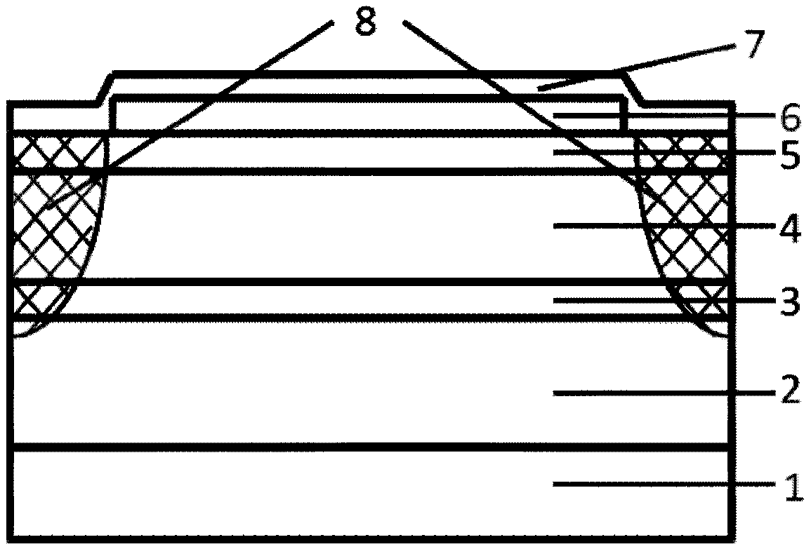
[0041] The GaAs-based epitaxial wafer described in this embodiment is a red semiconductor laser epitaxial wafer, and its structure is as attached figure 1 As shown, from bottom to top are substrate 1 , lower cladding layer 2 , active layer 3 , upper cladding layer 4 and contact layer 5 . Substrate 1 is N-type GaAs substrate; lower cladding layer 2 is N-type AlInP; active layer 3 is AlGaInP / GaInP quantum well structure; upper cladding layer 4 is P-type AlInP; contact layer 5 is P-type GaAs. This structure is a standard red semiconductor laser epitaxial structure. Because the cavity surface of the red semiconductor laser is more prone to defect absorption and COD occurs, it is necessary to make a non-absorbing window at the cavity surface. Generally, the diffusion of Zn impurities induces the interdiffusion of Al and Ga atoms in the quantum well to form a high bandgap window.

[0042] The solid-state zinc expansion method of a kind of GaAs base epitaxial wafer as described in e...


PUM

PropertyMeasurementUnit
thicknessaaaaaaaaaa
thicknessaaaaaaaaaa
thicknessaaaaaaaaaa

Abstract

The invention discloses a solid-state zinc-expanding method of a GaAs-based epitaxial wafer. A ZnO thin film is arranged on the GaAs epitaxial wafer to serve as a zinc source for performing zinc diffusion. The ZnO thin film is arranged on the GaAs epitaxial wafer in a sputtering mode. The temperature of zinc diffusion is 450-550 DEG C, the atmosphere of zinc diffusion is inert gas, preferably, theinert gas is nitrogen. The zinc diffusion source is the ZnO thin film, and is a solid-state source, so that the repeatability and the consistency of the diffusion process are relatively high. When the ZnO thin film is prepared by adopting the sputtering method, a damage layer can be formed on the surface of the epitaxial layer; and zinc atoms can easily enter the epitaxial layer along the damagedefects when zinc diffusion is carried out. An MOCVD reaction chamber is used for zinc diffusion, and the heat transfer mode adopts heat conduction, so that the temperature change of the epitaxial wafer is very fast, and the temperature uniformity of the whole epitaxial wafer is very high, thereby achieving very high diffusion uniformity and consistency.

Description

technical field [0001] The invention relates to a solid-state zinc expansion method for GaAs-based epitaxial wafers, belonging to the technical field of semiconductor technology. Background technique [0002] Thermal diffusion technology is an important step in the manufacturing process of semiconductor devices. Diffusing atoms undergo intense thermal motion at high temperatures, and the substances to be diffused on the surface move to the interior of the semiconductor through atomic gaps or displacements to achieve some special properties. Diffusion technology is relatively mature in silicon devices, and is widely used in semiconductor devices such as Schottky diodes, photodiodes, and photoresistors. In GaAs devices, Zn atoms become the most widely used diffusion source because of their small atomic radius, large diffusion coefficient, and low diffusion temperature. There are two main applications, one is to form a heavily doped P-type region by diffusion, which is used to...

Claims


Application Information

Patent Timeline
Patent Type & Authority Applications(China)
IPC IPC(8): H01L21/225
CPCH01L21/2258
Inventor 朱振张新徐现刚
Owner 潍坊华光光电子有限公司
Why Eureka
Try Eureka