Quinoxaline-fused dibenzosuberane based helicenes and organic light emitting diode element
A technology of quinoxaline fused dibenzocycloheptane helicene and light-emitting diodes, which is applied in the field of helicene derivative materials and organic light-emitting diode components, which can solve the problems of decreased stability and achieve good light emission Effects of efficiency and thermal stability, excellent fluorescent quantum effect and thermal stability
- Summary
- Abstract
- Description
- Claims
- Application Information
AI Technical Summary
Problems solved by technology
Method used
Image
Examples
Embodiment 1
[0040] Embodiment 1 quinoxaline fused dibenzocycloheptane helicene compound
[0041] According to the first embodiment of the present invention, a quinoxaline-fused dibenzoheptane helicene compound has the following general formula (1):
[0042]
[0043] Wherein, A has general formula (2), general formula (3a) or general formula (3b),
[0044]
[0045] Wherein, X is an oxygen atom, a sulfur atom, an amino group or -(CH 2 ) n , n is an integer from 0 to 2. R 1 and R 2 are independent hydrogen atoms, halogen atoms, general formula (4), general formula (5) or general formula (6),
[0046]
[0047] R 3 to R 15 One selected from independently hydrogen atom, halogen atom, cyano group, alkyl group, cycloalkyl group, alkoxy group, haloalkyl group, sulfanyl group, silyl group, alkenyl group, aryl group and amino group.
[0048]Here, the alkyl group is a substituted straight-chain alkyl group with 1 to 6 carbons, a straight-chained unsubstituted alkyl group, a substitut...
Embodiment 2
[0064] Embodiment 2 Organic Light Emitting Diode Element
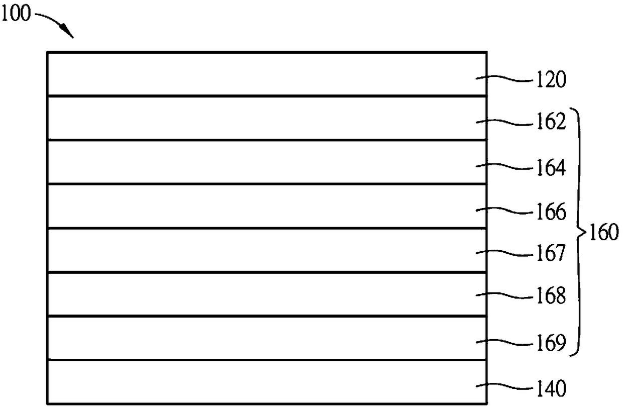
[0065] Please refer to figure 1 , an organic light emitting diode device 100 disclosed according to the second embodiment of the present invention includes a first electrode layer 120 , a second electrode layer 140 and an organic light emitting unit 160 . Wherein, the first electrode layer 120 may be a transparent electrode material, such as indium tin oxide (ITO), and the material of the second electrode layer 140 may be metal, transparent conductor or other suitable conductive material. However, the first electrode layer 120 can also be metal, transparent conductor or other suitable conductive material, and the second electrode layer 140 can also be a transparent electrode material. Specifically, at least one of the first electrode layer 120 and the second electrode layer 140 of this embodiment is a transparent electrode material. In this way, the light emitted by the organic light emitting unit 160 can be emitted ...
Embodiment 3
[0076] Embodiment 3 Organic Light Emitting Diode Element
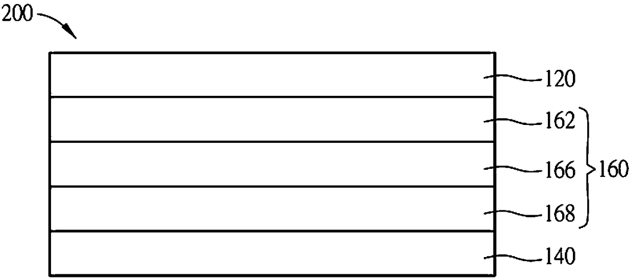
[0077] in addition, figure 2 It is a schematic cross-sectional view of an organic light emitting diode device 200 disclosed in the third embodiment of the present invention. The OLED device 200 is similar to the OLED device 100 , so the same components have the same features and functions, and are denoted by the same component symbols here, and will not be described again.
[0078] Please refer to figure 2 , and in this embodiment, the organic light emitting unit 160 may include a hole transport layer 162 , an organic light emitting layer 166 and an electron transport layer 168 , and the organic light emitting layer 166 is disposed between the hole transport layer 162 and the electron transport layer 168 .
PUM
| Property | Measurement | Unit |
|---|---|---|
| Glass transition temperature | aaaaa | aaaaa |
| Pyrolysis temperature | aaaaa | aaaaa |
| Oxidation potential | aaaaa | aaaaa |
Abstract
Description
Claims
Application Information
 - R&D
- Intellectual Property
- Life Sciences
- Materials
- Tech Scout
- Unparalleled Data Quality
- Higher Quality Content
- 60% Fewer Hallucinations
Browse by: Latest US Patents, China's latest patents, Technical Efficacy Thesaurus, Application Domain, Technology Topic, Popular Technical Reports.
© 2025 PatSnap. All rights reserved.Legal|Privacy policy|Modern Slavery Act Transparency Statement|Sitemap|About US| Contact US: help@patsnap.com


