Light absorption coating film as well as preparation method and application thereof
A technology of light absorption and light absorption rate, used in optics, nano-optics, optical components, etc., can solve the problems of easy degradation of coatings, complicated etching and laser treatment processes, and no wear resistance, and achieve a wide range of light absorption frequencies. , the effect of high absorption rate and low cost of raw materials
- Summary
- Abstract
- Description
- Claims
- Application Information
AI Technical Summary
Problems solved by technology
Method used
Image
Examples
Embodiment 1
[0070] Embodiment 1 Preparation of light-absorbing coating
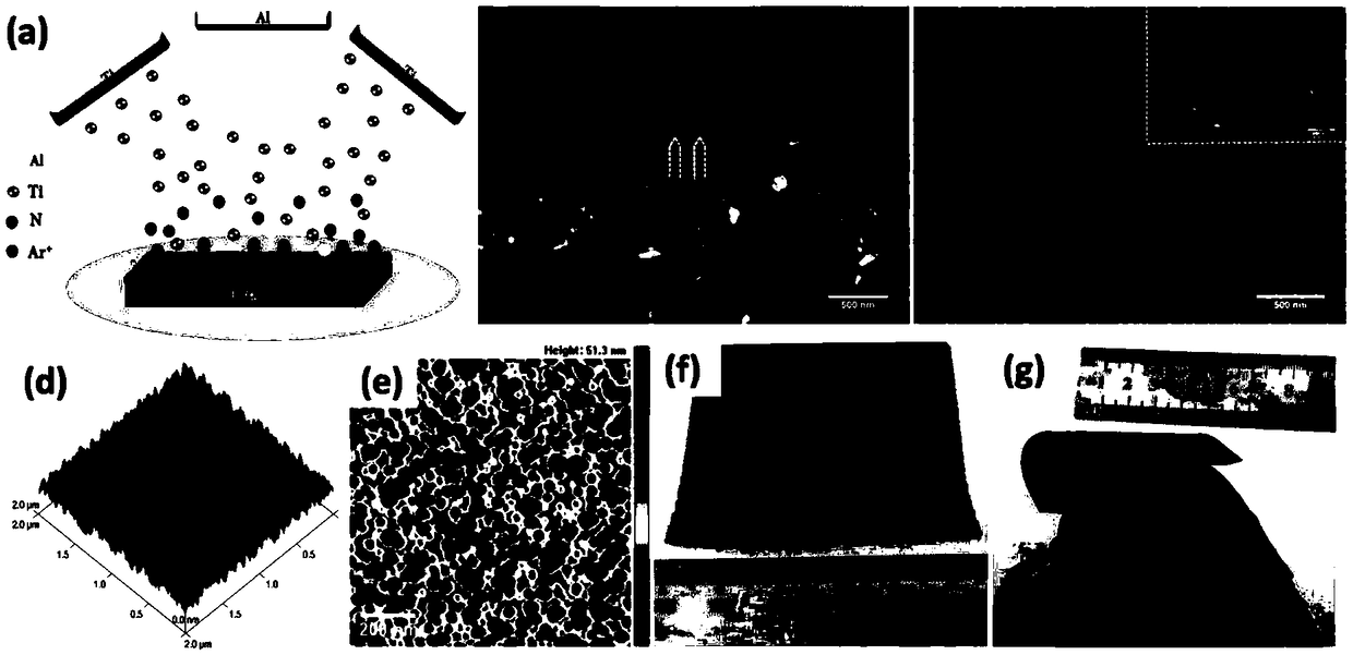
[0071] Vacuum equipment equipped with more than two magnetron sputtering target heads is used. The target materials are high-purity titanium target and high-purity aluminum target with a purity of 99.999%. The target size is titanium target: Φ100mm×10mm, aluminum target: Φ100mm×20mm . The two sputtering targets are connected to two DC power supplies respectively. The two targets are respectively inclined at 15° and point to the coating area together; the distance between the target and the substrate is 10 cm.
[0072] In order to ensure that the surface of the sample is clean, the substrate can be washed with ultrasonic water and absolute ethanol before coating.
[0073] 1 # sample preparation
[0074] With copper as the substrate, place the substrate copper in the coating area, and apply the vacuum degree of the vacuum device to 7.0×10 -4 Pa, feed 99.999% high-purity argon gas at a flow rate of 40 sccm until ...
Embodiment 2
[0088] Structural characterization of embodiment 2 light-absorbing coating
[0089] with 1 # The sample is typical, and its cross-sectional morphology is characterized by scanning electron microscopy, such as figure 1 (b) and figure 1 As shown in (c), figure 1 (b) The columnar crystal structure is clearly visible, the grain width is 30-50nm, the thickness is 800-900nm, and the columnar crystal structure with a grain width of about 50nm and a thickness of about 900nm accounts for a large proportion, about 70%-90 %.
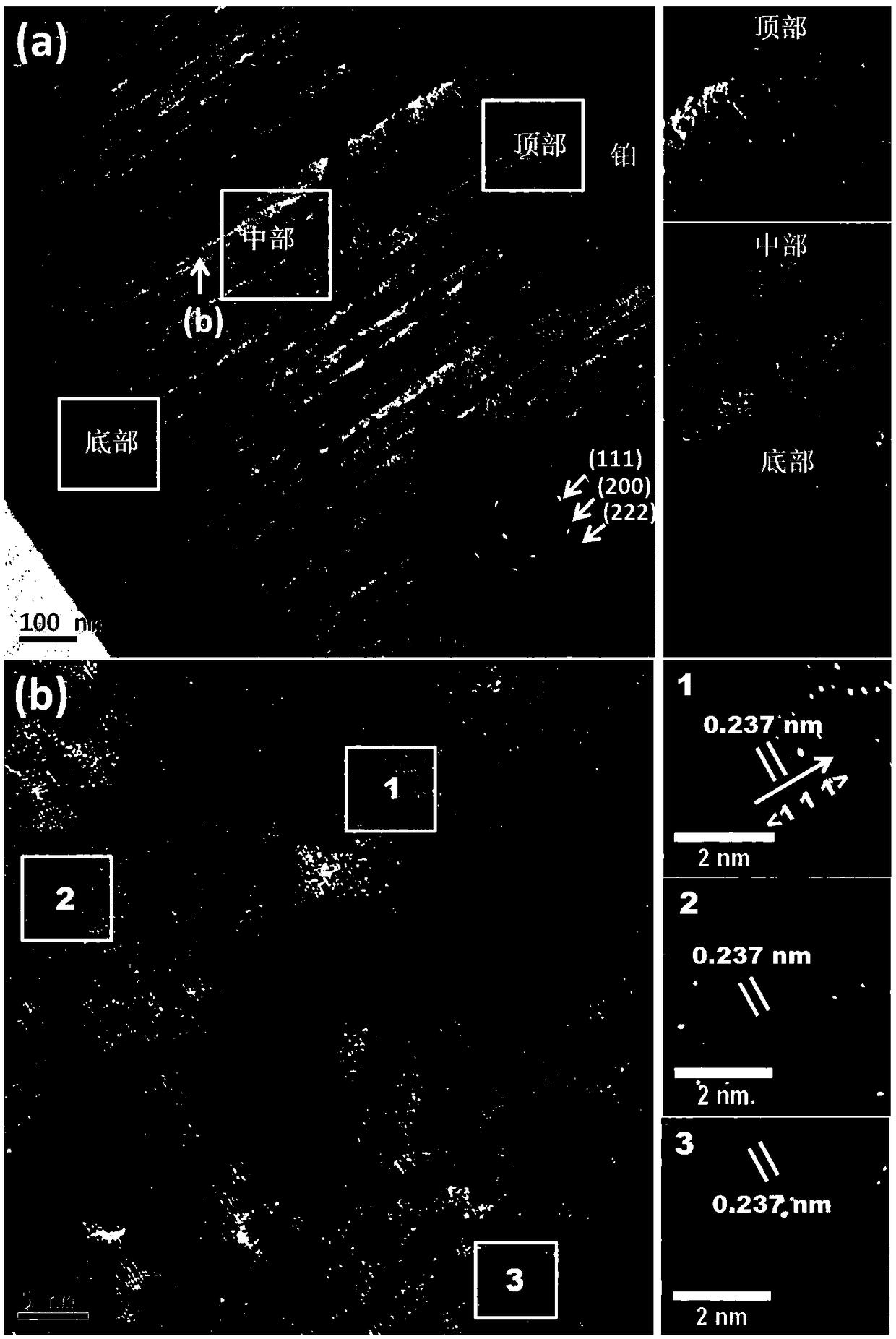
[0090] The structure was characterized by transmission electron microscopy, as figure 2 as shown, figure 2 In (a), the nano-layered structure at the bottom of the sample and the columnar crystal structure outside can be observed. The columnar crystal grains are about 50nm wide and about 900nm high; figure 2 In (b), the subgrain boundary structure inside the columnar grain can be observed, and the width of the subgrain boundary is about 0.237nm.
[0091] T...
Embodiment 3
[0102] Performance characterization of embodiment 3 light-absorbing coating
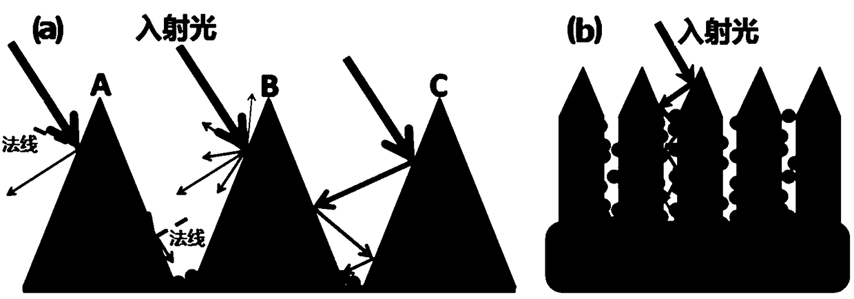
[0103] image 3 Schematic diagram of the light absorption principle of the light-absorbing coating of the present application, (a) is a schematic diagram of the process of inducing incident light to the interior of the coating on the coating surface, and (b) a schematic diagram of the process of light multiple reflections between grain boundaries to improve absorption.
PUM
| Property | Measurement | Unit |
|---|---|---|
| thickness | aaaaa | aaaaa |
| thickness | aaaaa | aaaaa |
| thickness | aaaaa | aaaaa |
Abstract
Description
Claims
Application Information
 - R&D Engineer
- R&D Manager
- IP Professional
- Industry Leading Data Capabilities
- Powerful AI technology
- Patent DNA Extraction
Browse by: Latest US Patents, China's latest patents, Technical Efficacy Thesaurus, Application Domain, Technology Topic, Popular Technical Reports.
© 2024 PatSnap. All rights reserved.Legal|Privacy policy|Modern Slavery Act Transparency Statement|Sitemap|About US| Contact US: help@patsnap.com


