Miniature ultra-wideband common mode noise suppression circuit

A common mode noise and suppression circuit technology, applied in circuits, electrical components, waveguide devices, etc., can solve the problems of deteriorating common mode noise suppression effect, inability to adapt, large size, etc., to maintain signal integrity and ensure signal integrity sexual effect

Active Publication Date: 2018-10-16
NO 55 INST CHINA ELECTRONIC SCI & TECHNOLOGYGROUP CO LTD
View PDF7 Cites 3 Cited by
  • Summary
  • Abstract
  • Description
  • Claims
  • Application Information

AI Technical Summary

Problems solved by technology

[0003] At present, the technologies used in common mode noise suppression circuits are mainly divided into three types: (1) Coil winding on ferrite, the disadvantage is that it is suitable for MHz frequency band, and the size is too large to adapt to modern miniaturized circuit systems to transmit Gbps high-speed digital Signal requirements; (2) Introducing a defective ground structure (DGS, Defect Ground Structure) on the reference ground plane of the coupled microstrip line is equivalent to introducing LC resonance on the common-mode noise loop path, thereby achieving GHz common-mode noise suppression, However, when the DGS structure is applied to multilayer circuits, if there is a metal plane under the DGS reference ground plane, the common mode noise suppression effect will be significantly deteriorated; (3) multilayer circuit technology, the main process technology involved is multilayer PCB Process and low temperature co-fired ceramic (LTCC, Low Temperature Co-Fired Ceramic) process

Method used


Image

  • Miniature ultra-wideband common mode noise suppression circuit
  • Miniature ultra-wideband common mode noise suppression circuit
  • Miniature ultra-wideband common mode noise suppression circuit

Examples


Embodiment Construction

[0019] The present invention will be further explained below in conjunction with the accompanying drawings and specific embodiments.

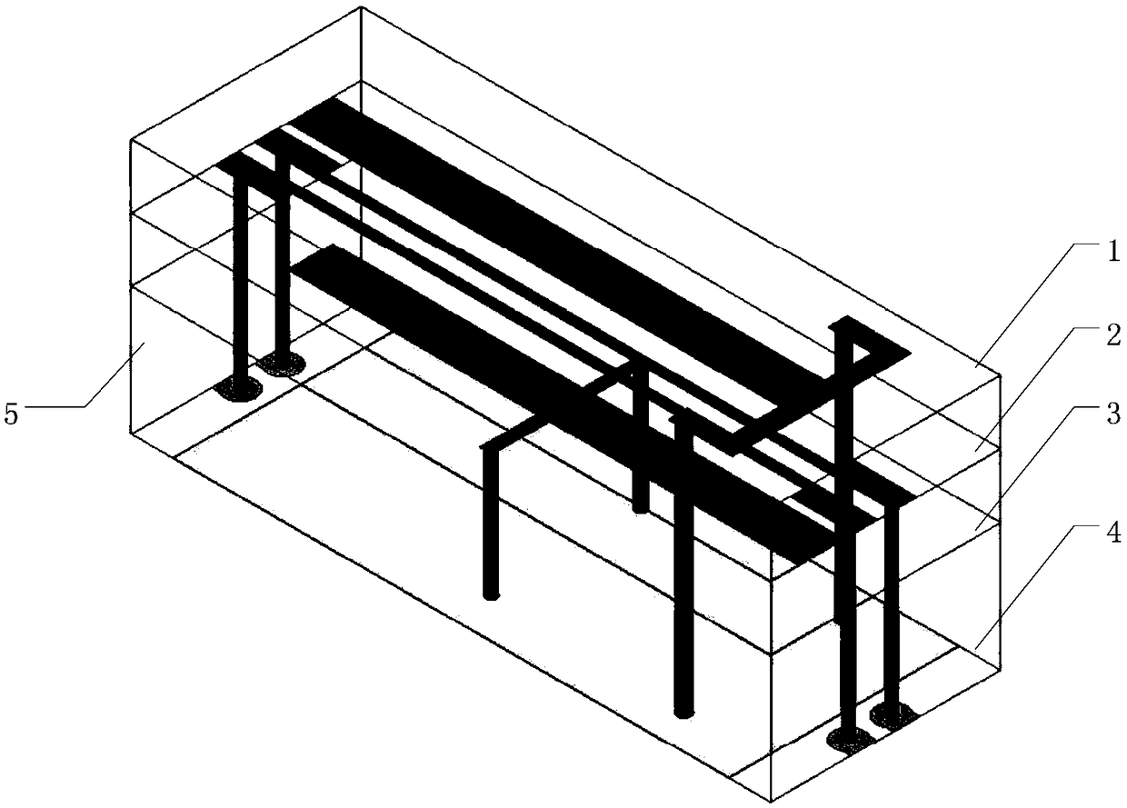
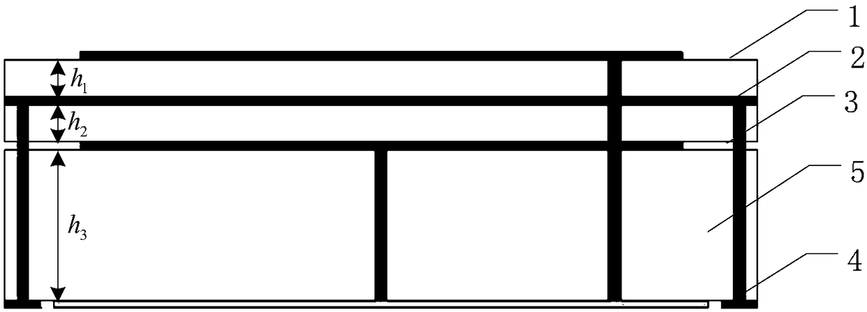
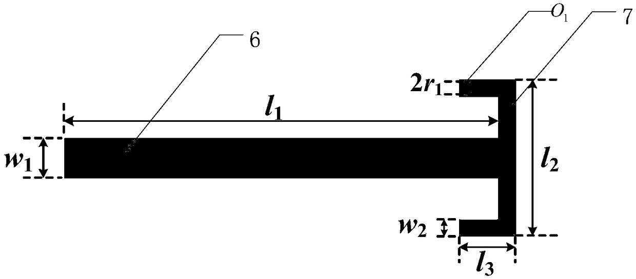
[0020] The common mode noise suppression circuit provided in this embodiment adopts multi-layer circuit technology, such as figure 1 and figure 2 Shown are the three-dimensional structural schematic diagram and side view of the common mode noise suppression circuit, respectively. The common mode noise suppression circuit has a four-layer circuit structure, all of which are made of metal, and copper / silver with less loss can be used to realize the actual circuit. The four-layer circuit includes a quarter-wavelength stepped impedance resonator layer 1, an embedded differentially coupled microstrip line layer 2, a half-wavelength resonator layer 3, and a reference ground layer 4; each layer is separated by a dielectric substrate 5; in this embodiment The LTCC process is adopted in the medium, the dielectric material is Dupont 951, and the relat...


PUM


Abstract

The invention discloses a miniature ultra-wideband common mode noise suppression circuit which comprises a quarter-wavelength stepped impedance resonator layer, an embedded differential coupling microstrip line layer, a half-wavelength resonator layer and a reference ground layer, wherein the layers are separated by dielectric substrates. The quarter-wavelength stepped impedance resonator layer comprises a quarter-wavelength stepped impedance resonator, wherein one end of the quarter-wavelength stepped impedance resonator is open circuit, and the other end of the quarter-wavelength stepped impedance resonator is connected with a first branch in parallel. The tail end of the first branch is connected with the reference ground layer through a metal via. The embedded differential coupling microstrip line layer comprises an embedded differential coupling microstrip line. The half-wavelength resonator layer comprises a half-wavelength resonator, and both ends of the half-wavelength resonator are open circuit. The circuit is applicable to the GHz frequency band, and the signal integrity of differential signal transmission can be ensured while common mode noise suppression is realized.

Description

technical field [0001] The invention belongs to the field of signal integrity, and in particular relates to a miniaturized ultra-wideband common-mode noise suppression circuit. Background technique [0002] In high-speed electronic circuit systems, differential signals are widely used to transmit high-speed digital signals due to their advantages of anti-noise and low electromagnetic interference. For example, high-speed interfaces such as HDMI, USB3.0, SATA-Ⅲ, and PCI-E all use differential wiring to transmit Gbps high-speed digital signals. However, in actual circuits, due to the asymmetry of differential wiring and the imbalance of differential signals, such as unequal rise and fall times, inconsistent amplitude and phase, common mode noise will be effectively excited, thereby affecting the transmission of differential signals; especially , when the common mode noise is transmitted to the cable together with the differential signal, it will cause serious electromagnetic ...

Claims


Application Information

Patent Timeline
Patent Type & Authority Applications(China)
IPC IPC(8): H01P1/212
CPCH01P1/212
Inventor 施永荣周鹏唐万春
Owner NO 55 INST CHINA ELECTRONIC SCI & TECHNOLOGYGROUP CO LTD
Why Eureka
Try Eureka