Method for preparing Mo-doped Al2O3 high-resistance film by atomic layer deposition

An atomic layer deposition and high-resistance technology, which is applied in coating, metal material coating process, gaseous chemical plating, etc. Excellent thermal stability, simple preparation process, smooth surface effect

Inactive Publication Date: 2018-09-28
XI'AN INST OF OPTICS & FINE MECHANICS - CHINESE ACAD OF SCI
View PDF2 Cites 2 Cited by
  • Summary
  • Abstract
  • Description
  • Claims
  • Application Information

AI Technical Summary

Problems solved by technology

[0004] The purpose of the present invention is to solve the deficiencies in the existing film preparation methods, and the inability to accurately control the film thickness and doping ratio, especially in the control of the film thickness to the atomic level and the simultaneous realization of large-area uniform growth. problem, provides an atomic layer deposition technique for the preparation of Mo-doped Al 2 o 3 The method of high-resistance film, the prepared film has strong adhesion, smooth surface, uniform thickness, and resistivity as high as 10 5 -10 11 Ω·cm, and good thermal stability

Method used


Image

  • Method for preparing Mo-doped Al2O3 high-resistance film by atomic layer deposition
  • Method for preparing Mo-doped Al2O3 high-resistance film by atomic layer deposition
  • Method for preparing Mo-doped Al2O3 high-resistance film by atomic layer deposition

Examples


Embodiment 1

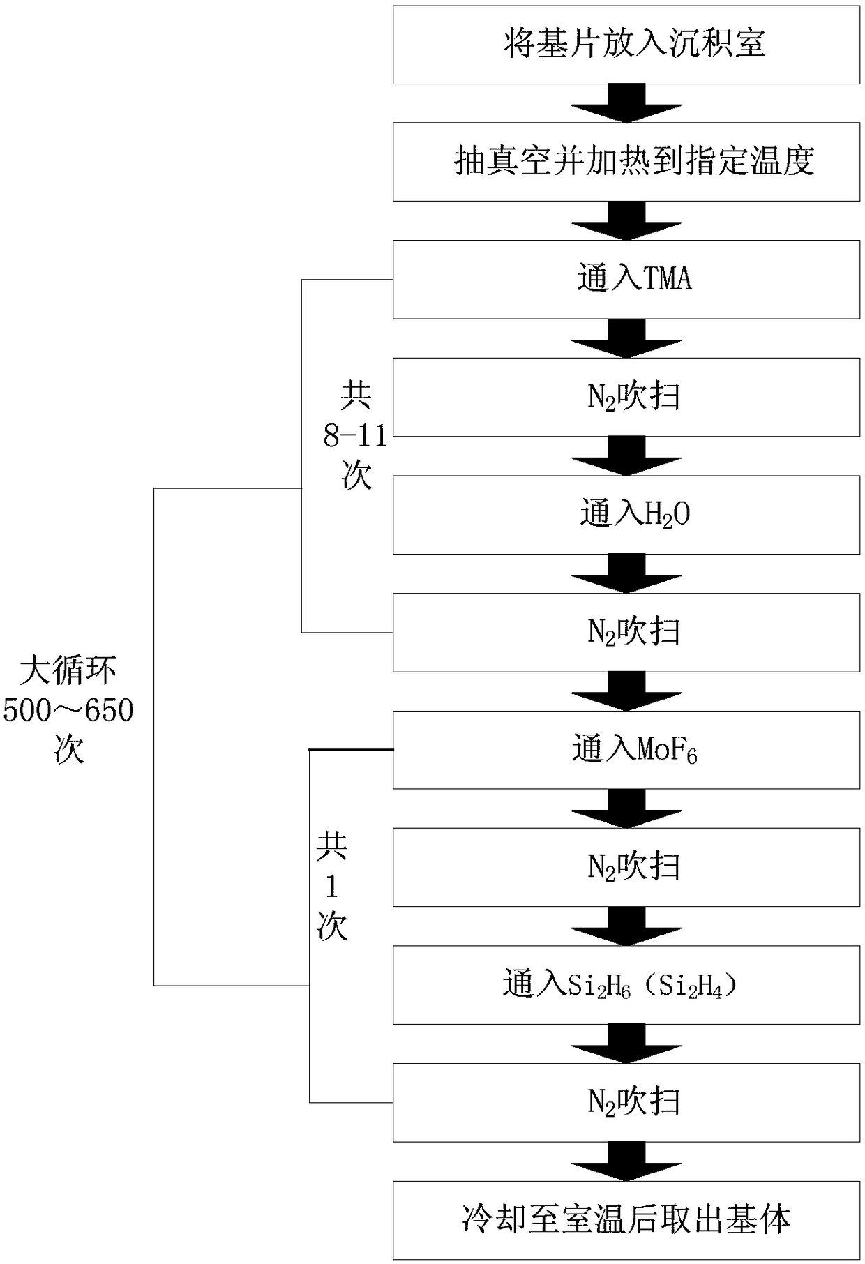
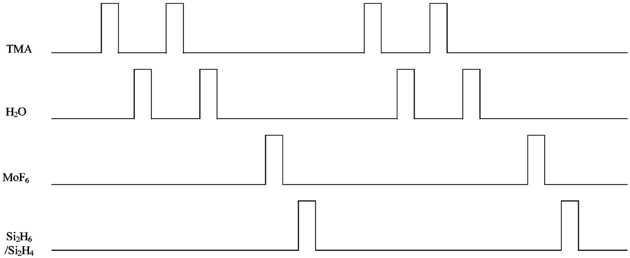
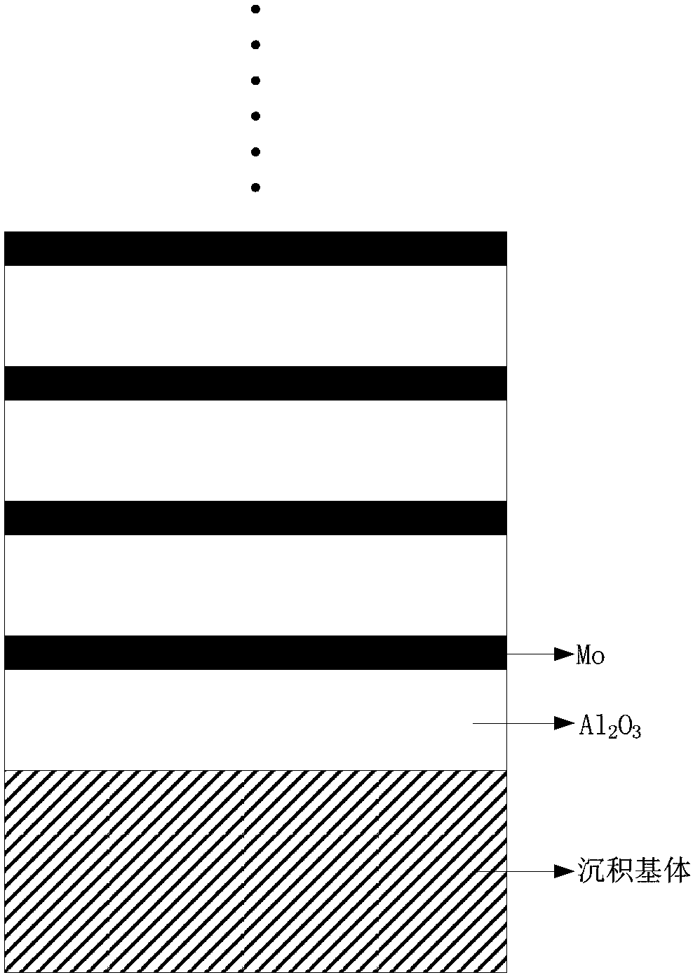
[0061] Put the substrate into the atomic layer deposition chamber and evacuate to 10 -2 Pa~10 -5 Pa, and the substrate is heated to 200°C to start Al 2 o 3 deposition, ie TMA / N 2 / H 2 O / N 2 =(0.1s / 3s / 0.1s / 3s), after 11 cycles, 1 Mo deposition, namely MoF 6 / N 2 / Si 2 h 6 (Si 2 h 4 ) / N 2 =(0.5s / 5s / 0.5s / 5s), 11 times Al 2 o 3 The deposition cycle and one Mo deposition constitute a large cycle. The deposition is stopped after 500 large cycles. After the temperature of the deposition chamber drops to room temperature, the deposition chamber is opened and the deposited Mo-doped Al 2 o 3 substrate of the film.

Embodiment 2

[0063] Put the substrate into the atomic layer deposition chamber and evacuate to 10 -2 Pa~10 -5 Pa, and the substrate is heated to 200°C to start Al 2 o 3 deposition, ie TMA / N 2 / H 2 O / N 2 =(0.1s / 3s / 0.1s / 3s), after 10 cycles, Mo deposition is carried out once, that is, M O f 6 / N 2 / Si 2 h 6 (Si 2 h 4 ) / N 2 =(0.5s / 5s / 0.5s / 5s), 10 Al2O3 deposition cycles and 1 Mo deposition is a large cycle, stop deposition after 550 large cycles, wait until the temperature of the deposition chamber drops to room temperature, open the deposition chamber, remove the deposited Mo-doped Al 2 o 3 substrate of the film.

Embodiment 3

[0065] Put the substrate into the atomic layer deposition chamber and evacuate to 10 -2 Pa~10 -5 Pa, and the substrate is heated to 200°C to start Al 2 o 3 deposition, ie TMA / N 2 / H2O / N 2 =(0.1s / 3s / 0.1s / 3s), after 9 cycles, Mo deposition is carried out once, that is, M O f 6 / N 2 / Si 2 h 6 (Si 2 h 4 ) / N 2 =(0.5s / 5s / 0.5s / 5s), 9 times Al 2 o 3 The deposition cycle and 1 Mo deposition are 1 large cycle. After 600 large cycles, the deposition is stopped. After the temperature of the deposition chamber drops to room temperature, the deposition chamber is opened, and the deposited Mo-doped Al 2 o 3 substrate of the film.


PUM

PropertyMeasurementUnit
electrical resistivityaaaaaaaaaa
surface roughnessaaaaaaaaaa
thicknessaaaaaaaaaa

Abstract

The invention relates to a method for preparing a Mo-doped Al2O3 high-resistance film by atomic layer deposition, and solves the problems of incapability of precisely controlling the film thickness and the mixing ratio, in particular existence of defects on the aspects of control of the film thickness precision reaching the atomic grade and synchronous realization of large-area uniform growth in the prior art. The method comprises the following steps: 1) a basal body is put in a deposition chamber; 2) the deposition chamber is vacuumized; and the basal body is heated; 3) 8-11 times of Al2O3 deposition circulation are performed; and single Al2O3 deposition comprises the following steps: 3.1) a precursor Al source is introduced into the deposition chamber; the Al source is exposed in the deposition chamber by set time; and the deposition chamber is purged; 3.2) a precursor oxygen source is introduced to obtain single-layer Al2O3; and 3.3) the deposition chamber is purged; 4) once Mo deposition is performed: 4.1) a precursor Mo source is introduced in the deposition chamber; and the deposition chamber is purged; 4.2) a reducing agent is introduced to obtain single-layer Mo metal simple substances; and 4.3) the deposition chamber is purged; and 5) the steps 3) and 4) are repeated by multiple times in sequence to obtain the Mo-doped Al2O3 high-resistance film.

Description

technical field [0001] The invention relates to a method for preparing a high-resistance thin film in the field of optoelectronic materials, in particular to a method for preparing Mo-doped Al by atomic layer deposition 2 o 3 High resistance film method. Background technique [0002] Since the 1980s, thin-film technology and thin-film materials have developed rapidly, and have achieved fruitful results in both academic and engineering applications, and have become one of the most active research fields in material science today. For a long time, the research hotspots of conductive thin films have focused on low-resistance thin films, especially the AZO thin films represented by Al-doped ZnO (aluminum-doped zinc oxide). There are few reports on the research of high-resistance thin films. Although by adjusting the Zn / Al ratio, the AZO film can also be prepared into a high-resistance film, but this AZO film has poor stability in a high-temperature working environment or afte...

Claims


Application Information

Patent Timeline
Patent Type & Authority Applications(China)
IPC IPC(8): C23C16/455C23C16/14C23C16/40
CPCC23C16/45529C23C16/14C23C16/403
Inventor 朱香平邹永星赵卫郭海涛陆敏许彦涛张文松
Owner XI'AN INST OF OPTICS & FINE MECHANICS - CHINESE ACAD OF SCI
Why Eureka
Try Eureka