
A scr device for input output port and power supply clamp

A technology of input and output ports and devices, which is applied in the field of ESD protection SCR device structure, can solve the problems of affecting the normal operation of devices, false triggering of SCR devices, and inability to use circuit input and output ports, etc.

Active Publication Date: 2020-10-23
UNIV OF ELECTRONICS SCI & TECH OF CHINA
View PDF5 Cites 0 Cited by
  • Summary
  • Abstract
  • Description
  • Claims
  • Application Information

AI Technical Summary

Problems solved by technology

[0014] The low trigger voltage SCR device structure can reduce the trigger voltage of the SCR device, but in normal operation, the SCR device can only be used for power supply V DD and V SS between the power supply clamping circuit, and cannot be used for the input and output ports of the circuit
Because, when the signal of the input and output port of the protected circuit changes, the voltage and current of the port will change with time, which may cause the SCR device to trigger falsely and affect the normal operation of the device.

Method used


Image

  • A scr device for input output port and power supply clamp
  • A scr device for input output port and power supply clamp
  • A scr device for input output port and power supply clamp

Examples


Embodiment 1

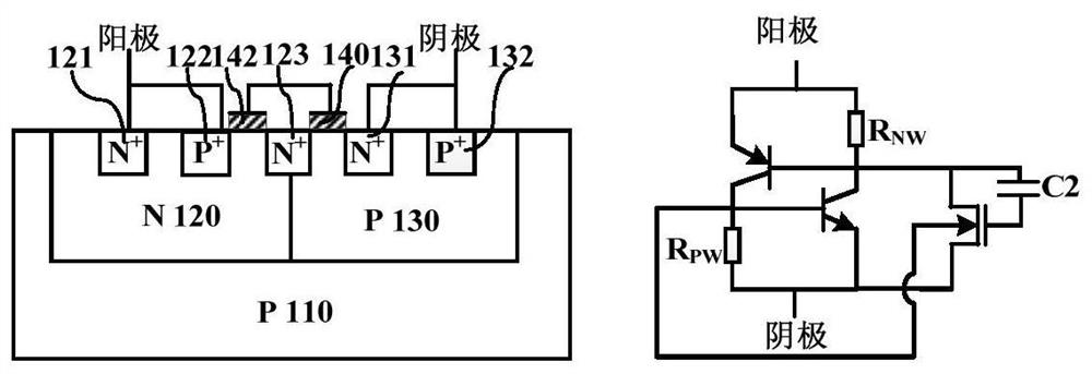
[0031] This embodiment provides an ESD protection SCR device used for input and output ports and power supply clamping. The structure and equivalent circuit of the SCR device are as follows: figure 2 As shown, its structure includes:

[0032] p-type silicon substrate 110;

[0033] A well region is formed on the p-type silicon substrate 110, the well region includes an n-type well region 120 and a p-type well region 130, and the well region 120 is adjacent to the well region 130;

[0034] The n-type well region 120 is provided with an n-type heavily doped region 121 and a p-type heavily doped region 122, and the n-type heavily doped region 121 and the p-type heavily doped region 122 are connected to the anode of the SCR device ;

[0035] The p-type well region 130 is provided with an n-type heavily doped region 131 and a p-type heavily doped region 132, and the n-type heavily doped region 131 and the p-type heavily doped region 132 are connected to the cathode of the SCR dev...

Embodiment 2

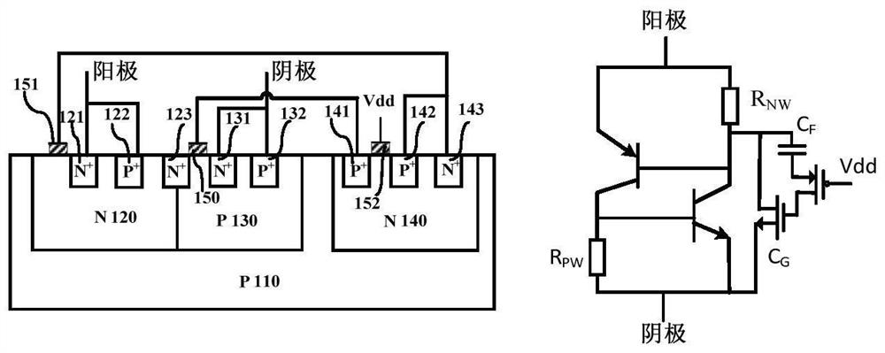
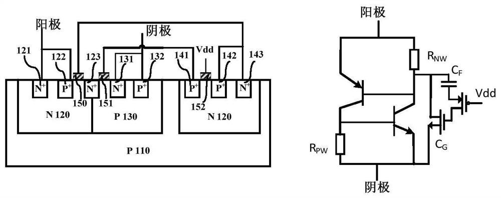
[0043] This embodiment provides an ESD protection SCR device used for input and output ports and power supply clamping. The structure and equivalent circuit of the SCR device are as follows: image 3 As shown, its structure is different from the structure in Embodiment 1 only in that the gate oxide layer region 150 on the silicon surface of the n-type well region 120 without the device structure region is arranged on the p-type heavily doped region 122 and the n-type heavily doped region on the silicon surface between the doped regions 123 . Thus, under the same ESD robustness, the structure shown in embodiment 2 has a smaller area than the structure in embodiment 1.

[0044] The SCR device consists of a main bleeder device and an auxiliary control device; the main bleeder device is composed of a parasitic PNP transistor, a parasitic NPN transistor, an external P-channel MOSFET device and a parasitic N-channel MOSFET device constitute. Among them, p-type heavily doped region...


PUM


Abstract

The invention belongs to the field of electrostatic discharge (ESD: Electrostatic Discharge) protection of integrated circuits, and specifically provides an SCR device for input and output ports and power supply clamping, which is used to simultaneously protect input and output ports and power supply clamping; the SCR device of the present invention The device includes a main discharge device and an auxiliary control device, wherein the auxiliary control device is used as a switch to control the main discharge device, and the auxiliary control device turns off the main discharge device during normal operation without affecting the protection of the circuit. Normal operation; when an ESD event comes, the auxiliary control device turns on the main discharge device and discharges the ESD current; at the same time, by designing the parameters of the internal RC path, the trigger voltage of the main discharge device can be reduced, and the trigger voltage adjustable.

Description

technical field [0001] The invention belongs to the field of electrostatic discharge (ESD: Electrostatic Discharge) protection of integrated circuits, relates to an ESD protection structure device, in particular to a novel ESD protection SCR device structure used for input and output ports and power supply clamping. Background technique [0002] Since the invention of the first bipolar transistor in 1947 and the birth of the first IC chip in 1958, electrostatic discharge has posed a growing threat to the reliability of IC chips. ESD destruction has the characteristics of concealment, latency, randomness and complexity. In the process of manufacturing, testing, packaging, transportation and use of IC chips, it is likely to be damaged by ESD, and the losses caused by this are shocking. Therefore, it is necessary to study the ESD protection scheme of IC chips. [0003] The design of the ESD protection scheme needs to ensure that when the electronic product or IC chip is workin...

Claims


Application Information

Patent Timeline
Patent Type & Authority Patents(China)
IPC IPC(8): H01L27/02
CPCH01L27/0262
Inventor 刘继芝何刚刘志伟赵建明
Owner UNIV OF ELECTRONICS SCI & TECH OF CHINA
Learn More