Surface plasmon-semiconductor heterojunction resonant optoelectronic device and preparation method thereof

A surface plasmon, optoelectronic device technology, applied in semiconductor devices, electrical components, circuits, etc., can solve the problems of complex, uncontrollable, poor "specificity" in the preparation process, achieve low-integration nano-optical devices, improve Quantum efficiency, effect of optimized structure

Inactive Publication Date: 2018-09-07
SOUTHEAST UNIV
View PDF0 Cites 0 Cited by
  • Summary
  • Abstract
  • Description
  • Claims
  • Application Information

AI Technical Summary

Problems solved by technology

The preparation process is complicated, the cost is high and the cycle is long. At the same time, it is difficult for the above technical means to realize semiconductor materials with adjustable aspect ratio, controllable density and variable orientation on the surface plasmon structure.
The crystal plane mismatch between different materials also leads to high interface loss and many uncertainties in the formed heterogeneous integrated optoelectronic devices, and the practicability and stability of the devices also need to be further explored
[0004] Therefore, there is an urgent need for a high-quality, stable and high-efficiency heterogeneous integrated optoelectronic device that can be prepared in large quantities, avoiding the poor "specificity" brought about by the traditional structural crystal plane technology (leading to the extremely easy generation of core-shell structures that cannot be realized. Light wave conduction), uncontrollable and other defects, so as to realize the direct and efficient coupling of surface plasmon polaritons and optical modes

Method used


Image

  • Surface plasmon-semiconductor heterojunction resonant optoelectronic device and preparation method thereof
  • Surface plasmon-semiconductor heterojunction resonant optoelectronic device and preparation method thereof
  • Surface plasmon-semiconductor heterojunction resonant optoelectronic device and preparation method thereof

Examples


Embodiment 1

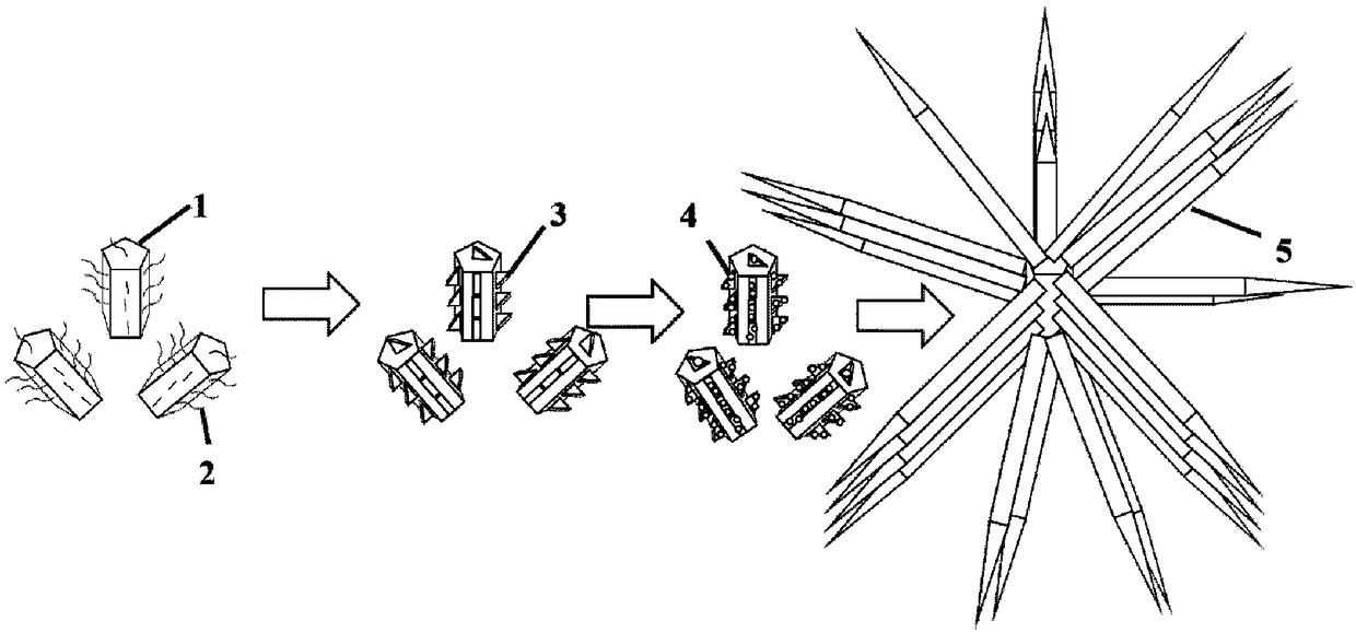
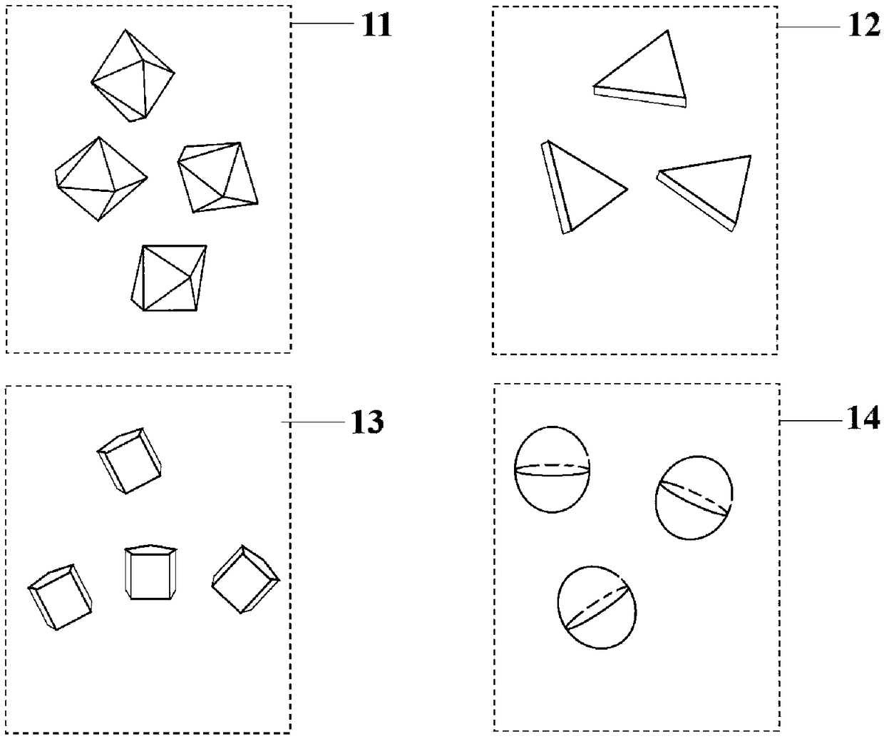
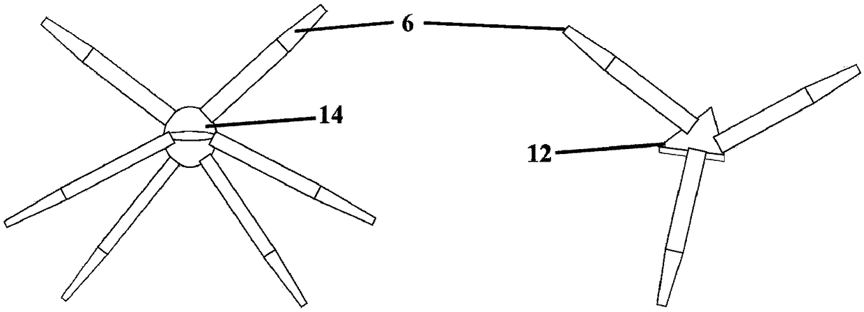
[0035] Embodiment 1: A surface plasmon-semiconductor heterojunction resonant optoelectronic device, the structure includes: the surface plasmon nanostructure is silver nano-decahedron, the size is 20nm; the surface ligand molecule is hexadecyltri Methyl ammonium bromide CTAB; the surface plasmon crystal plane structure is silver triangular plate, the size is 5nm; the semiconductor nanostructure seed crystal is zinc oxide; the one-dimensional semiconductor nanostructure is zinc oxide nanorod, the size is 500nm. The positional relationship is that hexadecyltrimethylammonium bromide CTAB is modified on the specific crystal face of the silver nano-decahedron, the silver triangular plate crystal face is bound to the cetyltrimethylammonium bromide CTAB, and the zinc oxide crystal The seed is located on the silver triangular plate crystal surface, the zinc oxide nanorod is located on the zinc oxide seed crystal, and each part forms a close contact.

[0036] The preparation method fol...

Embodiment 2

[0041] Embodiment 2: A surface plasmon-semiconductor heterojunction resonant photoelectric device, the structure includes: the surface plasmon nanostructure is a gold nanotriangular plate with a size of 60nm; the surface ligand molecule is polyvinylpyrrolidone PVP; the surface plasmon crystal plane structure is gold nanorods with a size of 10nm; the semiconductor nanostructure seed crystal is copper oxide; the one-dimensional semiconductor nanostructure is copper oxide nanocones with a size of 1000nm. The positional relationship is that the polyvinylpyrrolidone PVP is modified on the specific crystal face of the gold nanotriangular plate, the crystal face of the gold nanorod is bound on the polyvinylpyrrolidone PVP, and the copper oxide crystal is located on the crystal face of the gold nanorod. Above, the copper oxide nanocone is located on the copper oxide seed crystal, and each part forms a close contact.

[0042] The preparation method follows the steps below:

[0043] St...

Embodiment 3

[0047] Embodiment 3: A surface plasmon-semiconductor heterojunction resonant optoelectronic device, the structure includes: the surface plasmon nanostructure is a platinum nanorod with a size of 80nm; the surface ligand molecule is mercaptopropionic acid MPA; the surface The plasmonic crystal plane structure is platinum nanocube with a size of 20nm; the semiconductor nanostructure seed crystal is alumina; the one-dimensional semiconductor nanostructure is alumina nanorod with a size of 500nm. The positional relationship is that the mercaptopropionic acid MPA is modified on the specific crystal face of the platinum nanorod, the platinum nanocube crystal face is bound to the mercaptopropionic acid MPA, the alumina seed is located on the platinum nanocube crystal face, and the alumina nanorod is bound to the platinum nanocube crystal face. On the alumina seed crystal, and the parts form intimate contact.

[0048] The preparation method follows the steps below:

[0049] Step 1: S...


PUM

PropertyMeasurementUnit
Long axis sizeaaaaaaaaaa
Sizeaaaaaaaaaa
Sizeaaaaaaaaaa

Abstract

The present invention provides a surface plasmon-semiconductor heterojunction resonant optoelectronic device and a preparation method thereof. Surface ligand molecules (2) are modify on a surface plasmon nanostructure (1), a surface plasmon crystal face structure (3) is bound on surface ligand molecules (1), a semiconductor nanostructure seed crystal (4) is located on the surface plasmon crystal face structure (3), a one-dimensional semiconductor nanostructure (5) is located on the semiconductor nanostructure seed crystal, and portions form tight contact. The heterogeneous integrated materialsachieve matching of crystal lattices at the interfaces to greatly reduce loss caused by defects and rough crystal faces, achieve direct coupling of a surface plasmon mode and an optical mode and havea good appliance prospect in the fields of nanometer lasers, nanometer heat sources, photoelectric detection and photocatalysis.

Description

technical field [0001] The invention relates to the field of nanomaterials and integrated optical devices, in particular to a surface plasmon-semiconductor heterojunction resonant optoelectronic device and a preparation method thereof. Background technique [0002] With the continuous development of semiconductor theory, while pursuing the miniaturization and integration of devices, how to construct semiconductor optoelectronic devices with high quantum efficiency, low cost and mass production is currently a hot research direction, and has opened up a series of new fields of application. However, due to the limitation of the band gap of semiconductor nanomaterials and the recombination of photogenerated carriers, traditional optoelectronic devices based on semiconductor materials have defects such as limited response wavelength and low quantum efficiency, which lead to such devices in practicability, Reliability and cost limit its application range and further industrializa...

Claims


Application Information

Patent Timeline
IPC IPC(8): H01L31/101H01L31/0352H01L31/18
CPCH01L31/03529H01L31/101H01L31/18H01L31/035209H01L31/035281H01L31/109
Inventor 张彤王善江张晓阳
Owner SOUTHEAST UNIV
Why Eureka
Try Eureka