


Quick Research
Generate reliable direction feasibility study reports for your R&D in just a few steps.

Technical Q&A
Discover and master advanced knowledge NOW. Basics, ideas, possibilities, all at once.

Find Solutions
As an expert in R&D theories, this can generate solutions to your technical problems instantly.

Evaluate Feasibility
Analyze your overall solution with one click, know your potential R&D risks in advance.

Monitor Landscape
Get weekly tech updates, stay abreast of the latest tech innovations and key insights.
FinFET-based master-slave flip-flop
A flip-flop, master-slave technology, applied in the direction of pulse generation, electrical components, electric pulse generation, etc., can solve the problems of large area, large number of FinFET tubes, unfavorable low power consumption circuit design, etc.
- Summary
- Abstract
- Description
- Claims
- Application Information
AI Technical Summary
Problems solved by technology
Method used
Image

Examples
Embodiment 1
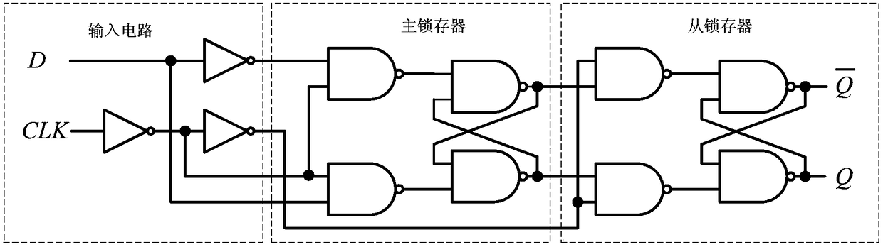
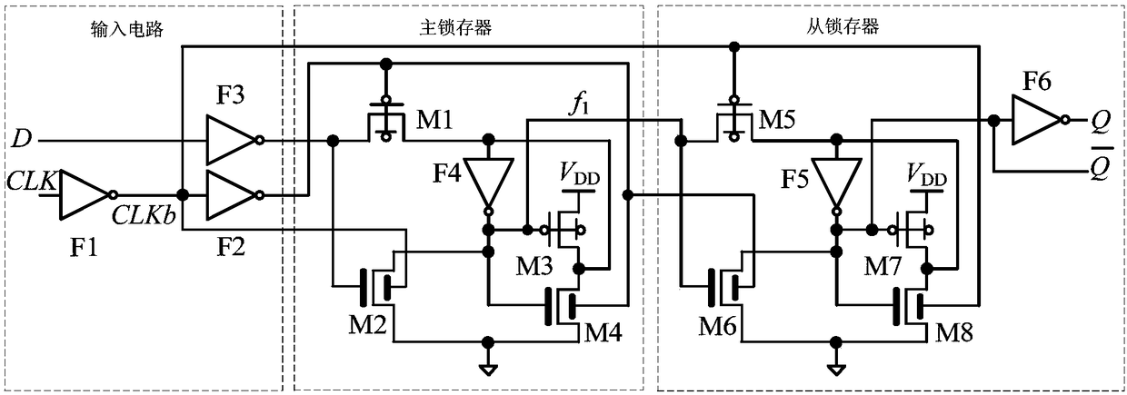
[0015] Embodiment one: if figure 2As shown, a master-slave flip-flop based on FinFET includes an input circuit, a master latch and a slave latch, and the input circuit includes a first inverter F1, a second inverter F2 and a third inverter F3 , the input end of the first inverter F1 is the clock input end of the input circuit, which is used to access the clock control signal CLK, the output end of the first inverter F1 is connected to the input end of the second inverter F2 and connected to end is the inverted clock output end of the input circuit, and is used to output the inverted signal CLKb of the clock control signal CLK, the output end of the second inverter F2 is the clock output end of the input circuit, and the input end of the third inverter F3 The data input terminal of the master-slave flip-flop is used to access the external data D, the output terminal of the third inverter F3 is the data output terminal of the input circuit, and the master latch includes the fir...
Embodiment 2
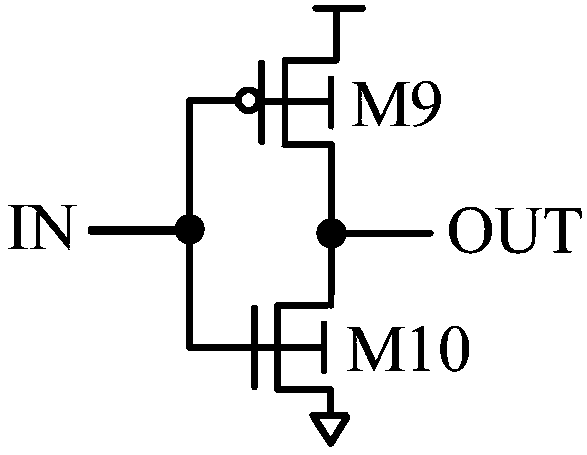
[0016] Embodiment 2: This embodiment is basically the same as Embodiment 1, the only difference is that in this embodiment, the first inverter F1 includes a ninth FinFET tube M9 and a tenth FinFET tube M10, and the ninth FinFET tube M9 is a P-type FinFET The tenth FinFET tube M10 is an N-type FinFET tube, the number of fins in the ninth FinFET tube M9 is 2, and the number of fins in the tenth FinFET tube M10 is 1; the source of the ninth FinFET tube M9 is connected to the power supply VDD, and the ninth FinFET tube M9 has The front gate of the FinFET tube M9, the back gate of the ninth FinFET tube M9, the front gate of the tenth FinFET tube M10, and the back gate of the tenth FinFET tube M10 are connected, and the connection terminal is the input terminal of the first inverter F1, and the connection terminal of the tenth FinFET tube M10 is connected to the input terminal of the first inverter F1. The drain of the ninth FinFET tube M9 is connected to the drain of the tenth FinFE...
PUM
 Abstract
Description
Claims
Application Information
 - R&D Engineer
- R&D Manager
- IP Professional
- Industry Leading Data Capabilities
- Powerful AI technology
- Patent DNA Extraction
Browse by: Latest US Patents, China's latest patents, Technical Efficacy Thesaurus, Application Domain, Technology Topic, Popular Technical Reports.
© 2024 PatSnap. All rights reserved.Legal|Privacy policy|Modern Slavery Act Transparency Statement|Sitemap|About US| Contact US: help@patsnap.com