Parallel white light organic electroluminescent device with six colors mixed and adjustable spectrum and its preparation method
An electroluminescent device, parallel technology, applied in the direction of electro-solid devices, semiconductor/solid-state device manufacturing, electrical components, etc., can solve the problems of white light device luminescence spectrum changes and other problems, achieve high efficiency, large half-peak width, and achieve display index Effect
- Summary
- Abstract
- Description
- Claims
- Application Information
AI Technical Summary
Problems solved by technology
Method used
Image
Examples
Embodiment 1
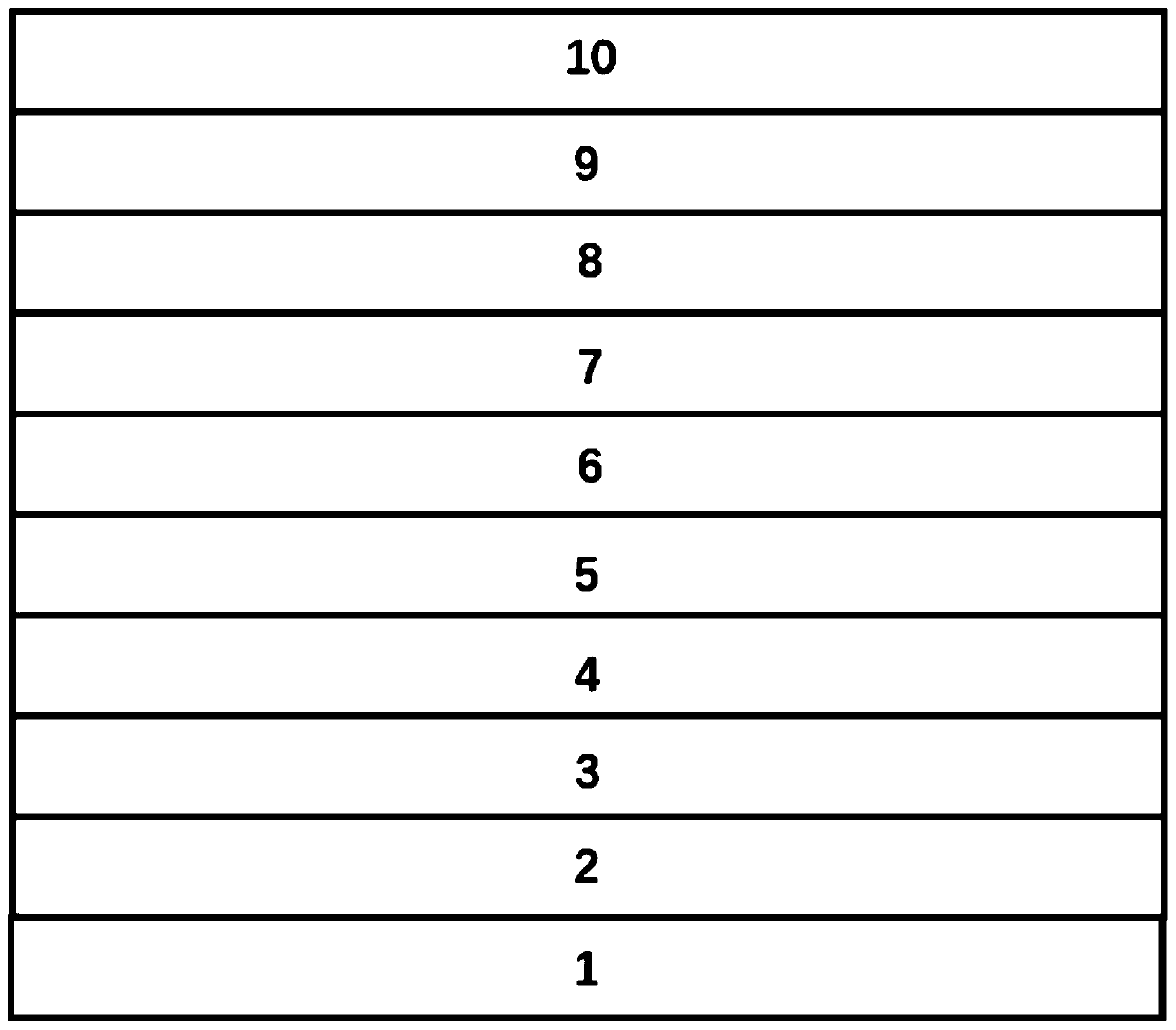
[0040] Clean the ITO first, dry it with nitrogen gas, and treat it with oxygen plasma for 2 minutes. In a vacuum of 1-5 x 10 -5 In Pa's coating system, MoO with a thickness of 8 nanometers is sequentially evaporated on the treated ITO electrode. 3 , 80 nm thick TAPC hole transport layer, 20 nm thick light emitting layer formed by six light emitting films, 40 nm PPT electron transport layer; and 1 nm LiF interface layer, and finally evaporated on LiF with discrete thickness 200nm metal Al electrode;
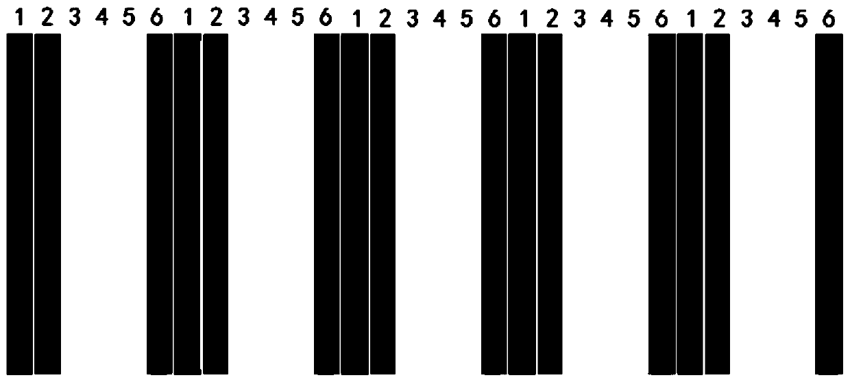
[0041] The combination of cycle units in the light-emitting layer is as follows: DSA-Ph doped with a weight ratio of 0.5% MADN, BCZ-TRZ with a weight ratio of 20% doped PPT, Ir(ppy) 3 Bepp doped at 6% by weight 2 , PO-01 Bepp doped with a weight ratio of 6% 2 , Ir(fbi)(acac) Bepp doped with 6% by weight 2 、Ir(bt) 2 Bepp doped at 6% by weight 2、 ;
[0042] MoO 3 , TAPC, MADN, Bepp 2 And the evaporation rate of PPT is controlled at 0.2 nanometers per second, DSA-Ph, BCZ-TR...
Embodiment 2
[0048] Clean the ITO first, dry it with nitrogen gas, and treat it with oxygen plasma for 2 minutes. In a vacuum of 1-5 x 10 -5 In Pa's coating system, MoO with a thickness of 8 nanometers is sequentially evaporated on the treated ITO electrode. 3 , 80 nm thick TAPC hole transport layer, 20 nm thick light emitting layer formed by six light emitting films, 40 nm PPT electron transport layer; and 1 nm LiF interface layer, and finally evaporated on LiF with discrete thickness 200nm metal Al electrode;
[0049] The combination of cycle units in the light-emitting layer is as follows: DSA-Ph doped with a weight ratio of 0.5% MADN, TCZ-TRZ with a weight ratio of 20% doped PPT, Ir(ppy) 3 Bepp doped at 6% by weight 2 , PO-01 Bepp doped with a weight ratio of 6% 2 , DCJTB Bepp doped with 1% by weight 2 、Ir(piq) 3 Bepp doped at 6% by weight 2 ;
[0050] MoO 3 , TAPC, MADN, Bepp 2 And PPT evaporation rate is controlled at 0.2 nanometers per second, DSA-Ph, TCZ-TRZ, Ir(ppy) 3 ,...
Embodiment 3
[0053] Clean the ITO first, dry it with nitrogen gas, and treat it with oxygen plasma for 2 minutes. In a vacuum of 1-5 x 10 -5 In Pa's coating system, MoO with a thickness of 8 nanometers is sequentially evaporated on the treated ITO electrode. 3 , 80 nm thick TAPC hole transport layer, 20 nm thick light emitting layer formed by six light emitting films, 40 nm PPT electron transport layer; and 1 nm LiF interface layer, and finally evaporated on LiF with discrete thickness 200nm metal Al electrode;
[0054] The combination of constituting the cycle unit in the light-emitting layer is as follows: DMAC-DPS is 30% by weight doped PPT, YDCZ-TRZ is 20% by weight doped PPT, Ir(ppy) 3 Bepp doped at 6% by weight 2 , PO-01 Bepp doped with a weight ratio of 6% 2 , DCJTB Bepp doped with 1% by weight 2 、Ir(piq) 3 Bepp doped at 6% by weight 2 ;
[0055] MoO 3 , TAPC, MADN, Bepp 2 And PPT evaporation rate is controlled at 0.2 nanometers per second, DMAC-DPS, YDCZ-TRZ, Ir(ppy) 3 ,...
PUM
| Property | Measurement | Unit |
|---|---|---|
| emission peak | aaaaa | aaaaa |
| thickness | aaaaa | aaaaa |
| thickness | aaaaa | aaaaa |
Abstract
Description
Claims
Application Information
 - R&D Engineer
- R&D Manager
- IP Professional
- Industry Leading Data Capabilities
- Powerful AI technology
- Patent DNA Extraction
Browse by: Latest US Patents, China's latest patents, Technical Efficacy Thesaurus, Application Domain, Technology Topic, Popular Technical Reports.
© 2024 PatSnap. All rights reserved.Legal|Privacy policy|Modern Slavery Act Transparency Statement|Sitemap|About US| Contact US: help@patsnap.com


