High reflection film with high damage threshold and preparation method thereof
A technology with high damage threshold and high reflection film, which is applied in the field of optics and can solve problems such as processing that does not consider heat conduction/accumulation
- Summary
- Abstract
- Description
- Claims
- Application Information
AI Technical Summary
Problems solved by technology
Method used
Image
Examples
Embodiment 1
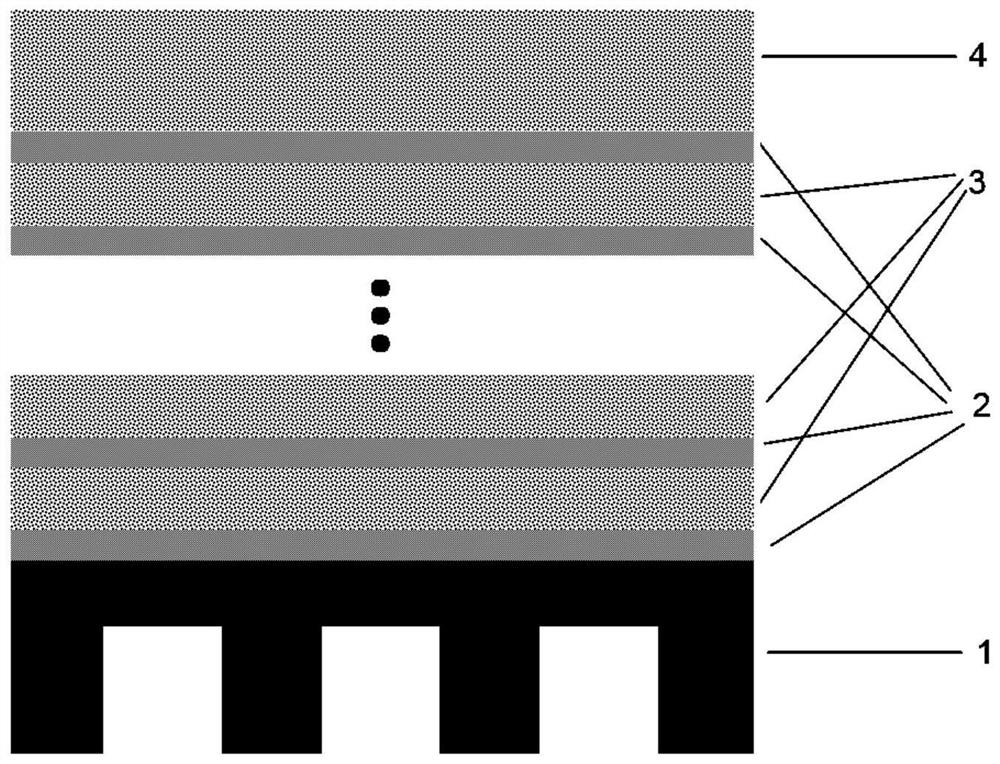
[0029] Embodiment 1: A high-reflection film with a high damage threshold, using crystalline silicon as a substrate, one of the surfaces of the substrate is evenly distributed with mesoporous silicon micro-wire arrays 1 with a pitch of the order of microns, and the other of the substrate is Several groups of high and low refractive index film pairs with an optical thickness of 1 / 4 wavelength are arranged on the surface, with the substrate surface as the inner side, and the high and low refractive index film pairs are sequentially composed of high refractive index film pairs with an optical thickness of 1 / 4 wavelength from the inside to the outside. Film 2, a low-refractive-index film 3 with an optical thickness of 1 / 4 wavelength; the outermost high- and low-refractive-index film pair is followed by a high-refractive index film 2 with an optical thickness of 1 / 4 wavelength and a film with an optical thickness of 1 / 2 wavelength Low refractive index film4.
Embodiment 2
[0031] Based on the above-mentioned high reflection film, a method for preparing a high damage threshold high reflection film is also provided, comprising the following steps:
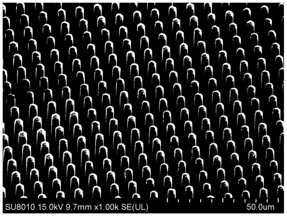
[0032] 1). Using crystalline silicon as the substrate, the crystalline silicon can be a double-sided polished heavily doped wafer (resistivity<0.01Ω·cm), and then perform template-assisted chemical silicon etching on one surface of the crystalline silicon, The thickness of the unetched silicon is about 100 microns, and a silicon micron line array with a pitch in the order of microns and a mesoporous surface is obtained. The preparation principle and corrosion process conditions can refer to other invention patents, the patent application number is 201610183558.7.
[0033] 2). On the other surface of the uncorroded substrate, use atomic layer deposition technology to grow a high refractive index film, and then use the sol-gel method to grow a low refractive index film. The optical thickness of the high ...
Embodiment 3
[0047] Compared with the second embodiment, the difference lies in the high reflection of different target wavelengths, and the optical thickness of the high and low refractive index film needs to be adjusted accordingly. The preparation process and parameters of silicon micro-wire arrays are consistent, but the growth experimental parameters of high and low refractive index films need to be changed according to the experimental results.
PUM
| Property | Measurement | Unit |
|---|---|---|
| electrical resistivity | aaaaa | aaaaa |
| thickness | aaaaa | aaaaa |
| reflectance | aaaaa | aaaaa |
Abstract
Description
Claims
Application Information
 - R&D
- Intellectual Property
- Life Sciences
- Materials
- Tech Scout
- Unparalleled Data Quality
- Higher Quality Content
- 60% Fewer Hallucinations
Browse by: Latest US Patents, China's latest patents, Technical Efficacy Thesaurus, Application Domain, Technology Topic, Popular Technical Reports.
© 2025 PatSnap. All rights reserved.Legal|Privacy policy|Modern Slavery Act Transparency Statement|Sitemap|About US| Contact US: help@patsnap.com


