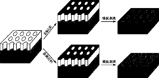
Manufacturing method of metal nanostructure array based on interface induction growth
A metal nanostructure and metal-inducing technology, which is applied in the direction of nanotechnology, nanotechnology, nanotechnology, etc. for materials and surface science, to achieve the effects of good controllability, simple process, and easy large-scale preparation
- Summary
- Abstract
- Description
- Claims
- Application Information
AI Technical Summary
Problems solved by technology
Method used
Image
Examples
Embodiment 1
[0022] (1) Soak the silicon wafer in a mixed solution of concentrated sulfuric acid and hydrogen peroxide at 90°C for 1 hour, then ultrasonically clean it in propanol, ethanol, and deionized water for more than 15 minutes, then rinse it with a large amount of deionized water, and finally Blow dry with nitrogen.
[0023] (2) Drop a drop of water on the cleaned silicon wafer surface, and adhere the ultra-thin porous alumina template supported by polymethyl methacrylate (PMMA) to the silicon surface. Then the sample was soaked in propanol solution for 5-10 minutes, the PMMA layer was removed, the template was transferred to the silicon substrate, washed once with clean propanol solution, and dried in the air.
[0024] (3) The adhesion between the porous alumina template and the substrate is weak, and the sample is left to stand for several hours to further relax the adhesion between the template and the substrate.
[0025] (4) The substrate with the alumina template on the surfa...
Embodiment 2
[0028] (1) Soak the silicon wafer in a mixed solution of concentrated sulfuric acid and hydrogen peroxide at 90°C for 1 hour, then ultrasonically clean it in propanol, ethanol, and deionized water for more than 15 minutes, then rinse it with a large amount of deionized water, and finally Blow dry with nitrogen.
[0029] (2) Drop a drop of water on the surface of the cleaned silicon wafer, and adhere the ultra-thin porous alumina template supported by PMMA to the surface of the silicon surface. Then the sample was soaked in propanol solution for 5-10 minutes, the PMMA layer was removed, the template was transferred to the silicon substrate, washed once with clean propanol solution, and dried in the air.
[0030] (3) The adhesion between the porous alumina template and the substrate is weak, and the adhesion between the template and the silicon substrate is strengthened by low-temperature annealing. The low-temperature annealing is carried out by a heating plate. 4 hours.
[0...
Embodiment 3
[0034] (1) Soak the silicon wafer in a mixed solution of concentrated sulfuric acid and hydrogen peroxide at 90°C for 1 hour, then ultrasonically clean it in propanol, ethanol, and deionized water for more than 15 minutes, then rinse it with a large amount of deionized water, and finally Blow dry with nitrogen.
[0035] (2) Drop a drop of water on the surface of the cleaned silicon wafer, and adhere the ultra-thin porous alumina template supported by PMMA to the surface of the silicon surface. Then the sample was soaked in propanol solution for 5-10 minutes, the PMMA layer was removed, the template was transferred to the silicon substrate, washed once with clean propanol solution, and dried in the air.
[0036] (3) The adhesion between the porous alumina template and the substrate is weak, and the sample is left to stand for several hours to further relax the adhesion between the template and the substrate.
[0037] (4) The substrate with the alumina template on the surface w...
PUM
| Property | Measurement | Unit |
|---|---|---|
| Thickness | aaaaa | aaaaa |
Abstract
Description
Claims
Application Information
 - R&D
- Intellectual Property
- Life Sciences
- Materials
- Tech Scout
- Unparalleled Data Quality
- Higher Quality Content
- 60% Fewer Hallucinations
Browse by: Latest US Patents, China's latest patents, Technical Efficacy Thesaurus, Application Domain, Technology Topic, Popular Technical Reports.
© 2025 PatSnap. All rights reserved.Legal|Privacy policy|Modern Slavery Act Transparency Statement|Sitemap|About US| Contact US: help@patsnap.com


